
Method for modifying appearances of side walls of through holes

A modification method and morphology technology, which is applied in the field of through-hole sidewall morphology modification, can solve the problems of low quality of through-silicon holes and serious leakage phenomenon, and achieve the effects of reducing roughness, optimizing oxidation process parameters, and fast oxidation rate

Active Publication Date: 2014-03-05
ADVANCED MICRO FAB EQUIP INC CHINA
View PDF4 Cites 0 Cited by
  • Summary
  • Abstract
  • Description
  • Claims
  • Application Information

AI Technical Summary

Problems solved by technology

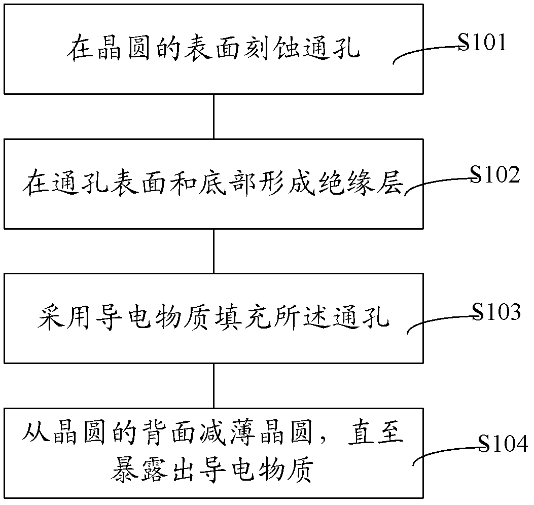
[0010] However, the quality of the TSVs formed by the existing process is low, and the leakage phenomenon is serious

Method used


Image

  • Method for modifying appearances of side walls of through holes
  • Method for modifying appearances of side walls of through holes
  • Method for modifying appearances of side walls of through holes

Examples


Embodiment Construction

[0027] The inventors conducted research on through-silicon via products with severe leakage, and analyzed the cross-section of the through-silicon via with a scanning electron microscope, and found that the appearance of the through-hole formed by the existing process is as follows: Image 6 Shown are scalloped, serrated or corrugated with high roughness. Form an insulating layer on the surface of a shell-shaped, jagged or corrugated through-hole with high roughness, and then fill it with a conductive substance. The uniformity of the insulating layer is difficult to control, so that the conductive substance along the thinner position of the insulating layer Diffusion into the wafer, resulting in serious leakage of TSV products.

[0028] The inventor further analyzed the existing through-silicon via technology and found that the formation process of the through-silicon via interconnection structure usually uses a plasma etching process to etch the through-hole. Since the thickn...


PUM


Abstract

The invention relates to a method for modifying appearances of side walls of through holes, which comprises the following steps of: providing a silicon substrate, wherein the through holes are formed in the silicon substrate, and the side wall of each through hole has first roughness; performing oxidation on projecting parts by adopting an oxidation technology aiming at the projecting parts of the side walls of the through holes; and performing bath washing on the oxidated silicon substrate by adopting a wet etching solution to form the side walls of the through holes, which have second roughness respectively, wherein the second roughness is lower than the first roughness. The through holes formed by the method for modifying the appearances of the side walls of the through holes are high in quality.

Description

technical field [0001] The invention relates to the field of semiconductor manufacturing, in particular to a method for modifying the shape of the side wall of a through hole. Background technique [0002] In the past forty years, the research, development and production of microelectronic chips have been carried out along the prediction of Moore's Law; until 2008, companies such as Intel have begun to use 45nm to 50nm chips in the mass production of memory chips Line width processing technology. [0003] According to the prediction of Moore's Law, in order to further improve the integration level of the chip, it is necessary to use a processing technology with a line width of 32 nanometers or even 22 nanometers. However, the 32nm or 22nm processing technology not only encounters the limitations of lithography equipment and process technology, but also has unresolved problems such as cell stability, signal delay, and CMOS circuit feasibility. [0004] For this reason, the ...

Claims


Application Information

Patent Timeline
Patent Type & Authority Patents(China)
IPC IPC(8): H01L21/768
Inventor 黄智林严利均
Owner ADVANCED MICRO FAB EQUIP INC CHINA
Learn More