Resistive random access memory unit and memorizer

A technology of random storage and resistive storage, which is applied in the direction of electrical components, semiconductor devices, electric solid devices, etc., can solve the problems of three-dimensional high-density integration of unfavorable resistive random access memory, and achieve the reduction of process complexity, the realization of simple process, and the realization of Effect of rectification characteristics

Active Publication Date: 2014-01-29
INST OF MICROELECTRONICS CHINESE ACAD OF SCI
View PDF6 Cites 0 Cited by
  • Summary
  • Abstract
  • Description
  • Claims
  • Application Information

AI Technical Summary

Problems solved by technology

[0007] In the process of realizing the present invention, the inventor realized that the following technical problems existed in the prior art: in the resistive memory cell with 1D1R structure using PN junction as the gating unit, due to the need for additional doping and high-temperature activation process, there is no Conducive to three-dimensional high-density integration of resistive random access memory

Method used


Image

  • Resistive random access memory unit and memorizer
  • Resistive random access memory unit and memorizer
  • Resistive random access memory unit and memorizer

Examples


Embodiment Construction

[0030] In order to make the object, technical solution and advantages of the present invention clearer, the present invention will be described in further detail below in conjunction with specific embodiments and with reference to the accompanying drawings.

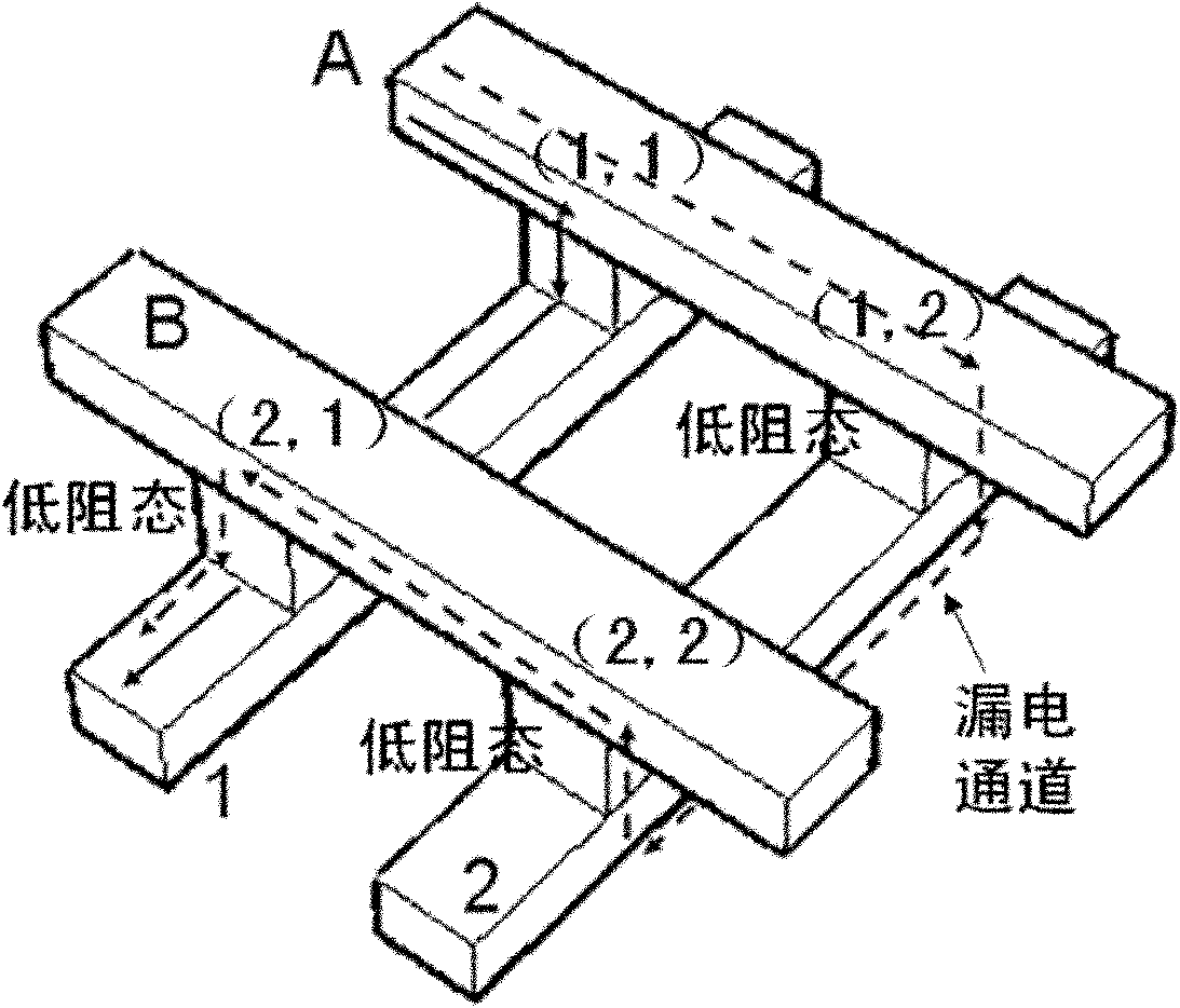
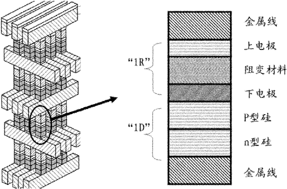
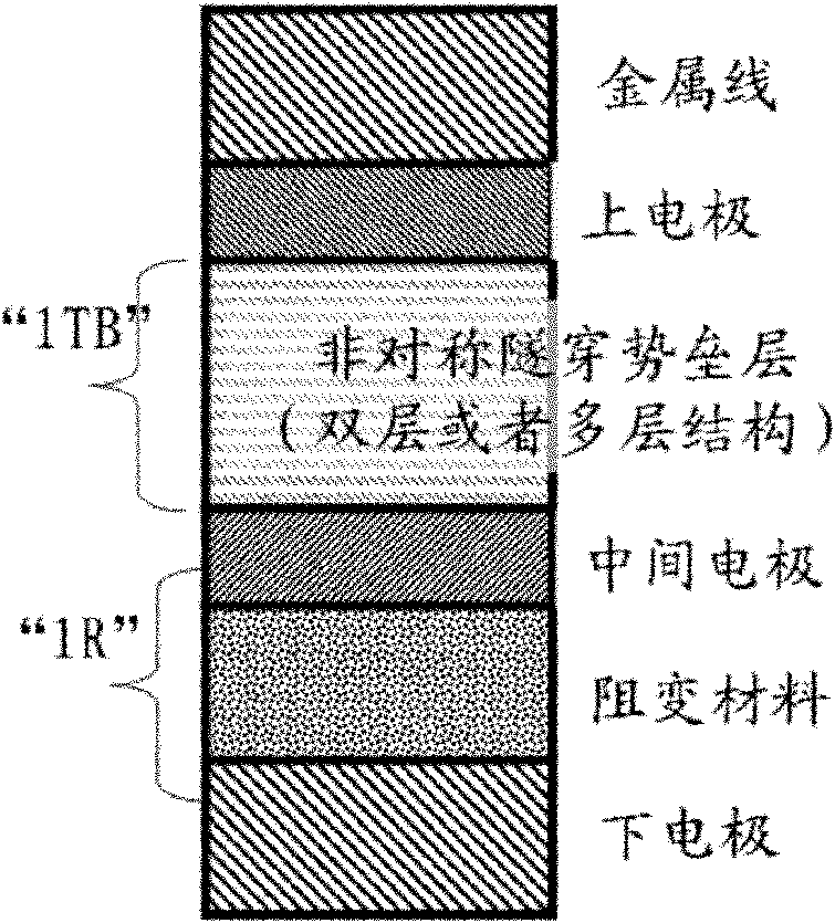
[0031] In an exemplary embodiment of the present invention, a resistive random access memory cell is provided. The memory cell is composed of an upper electrode, a resistive functional layer, an intermediate electrode, an asymmetric tunneling barrier layer and a lower electrode, wherein the upper electrode, the resistive functional layer and the intermediate electrode form a resistive memory part, and the intermediate electrode, the asymmetrical tunnel The through-barrier layer and the lower electrode constitute a gating function part, and the resistive memory part and the gating function part share the middle electrode. The gate function part can be located above or below the resistive memory part. If the gate function par...


PUM


Abstract

The present disclosure provides a resistive random memory cell and a resistive random memory. The resistive random memory cell comprises an upper electrode, a resistive layer, an intermediate electrode, an asymmetric tunneling barrier layer, and a lower electrode. The upper electrode, the resistive layer, and the intermediate electrode constitute a resistive storage portion. The intermediate electrode, the asymmetric tunneling barrier layer, and the lower electrode constitute a selection portion. The resistive storage portion and the selection portion share the intermediate electrode. The selection portion may be disposed above or under the resistive storage portion. The asymmetric tunneling barrier layer comprises at least two materials having different barrier heights, and is configured for rectifying forward tunneling current and reverse tunneling current flowing through the resistive random memory cell. The present disclosure uses the asymmetric tunneling barrier layer for rectifying, so as to enable selection of the resistive random memory cell. The method for manufacturing the asymmetric tunneling barrier layer does not involve doping or high-temperature annealing processes, and the thickness of the asymmetric tunneling barrier layer is relatively small, which helps 3D high-density integration of the resistive random memory.

Description

technical field [0001] The invention belongs to the technical field of microelectronics and memory, and in particular relates to a resistive variable random memory unit and memory for high-density data storage. Background technique [0002] Resistive random access memory (resistive random access memory, referred to as RRAM), as an emerging non-volatile storage technology, has great advantages in terms of cell area, device density, power consumption, programming / erasing speed, 3D integration and multi-value implementation, etc. Compared with FLASH, it has great advantages in many aspects, and has been highly concerned by large companies and research institutes at home and abroad. The continuous progress of resistive memory technology makes it one of the most powerful competitors for mainstream products in the future non-volatile memory technology market. [0003] Resistive memory has a simple cell structure of electrode / insulating layer / electrode. Therefore, the 1R cross-arr...

Claims


Application Information

Patent Timeline
Patent Type & Authority Patents(China)
IPC IPC(8): H01L45/00H01L27/24
CPCH01L27/2409H01L27/2463H10B63/20H10B63/80
Inventor 霍宗亮刘明张满红王艳花龙世兵
Owner INST OF MICROELECTRONICS CHINESE ACAD OF SCI
Why Eureka
Try Eureka