Power diode

A power diode and base technology, applied in the direction of electrical components, circuits, semiconductor devices, etc., to reduce substrate leakage, avoid punch-through, and improve reverse withstand voltage

Active Publication Date: 2012-08-01
SHANGHAI HUAHONG GRACE SEMICON MFG CORP
View PDF5 Cites 3 Cited by
  • Summary
  • Abstract
  • Description
  • Claims
  • Application Information

AI Technical Summary

Problems solved by technology

[0003] Common diodes, such as figure 1 The structure shown, due to the existence of parasitic triode devices, has a large substrate leakage when working in the forward direction

Method used


Image

  • Power diode
  • Power diode
  • Power diode

Examples


Embodiment Construction

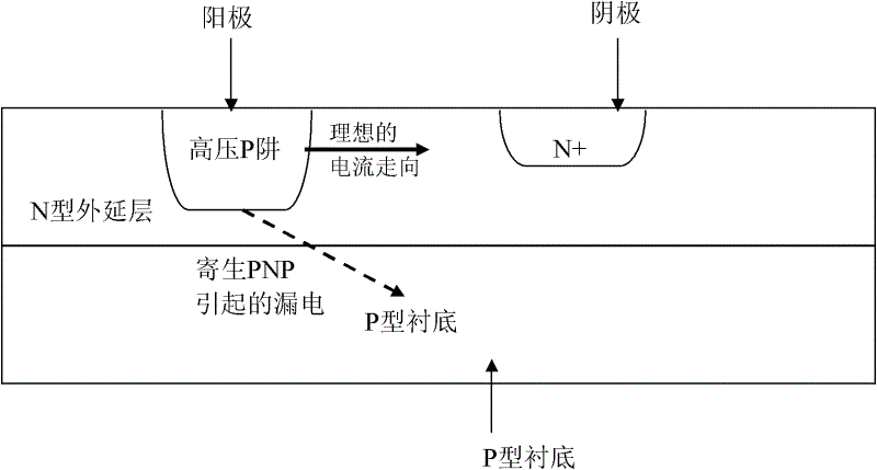
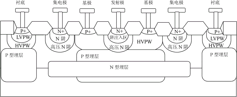
[0016] In the power diode of the NPN structure of the present invention, the base and the collector in the NPN structure are connected as the anode of the power diode, and the emitter is used as the cathode of the power diode. On the basis of the existing NPN structure, a well injection region is added under the emission region of the emitter end. The conductivity type of the well injection region is the same as that of the emission region, but the impurity concentration is lower than that of the emission region, which is used to improve the device. reverse withstand voltage. In order to prevent the punch-through problem between the collector and the emitter, a buried layer is provided on the substrate below the base. The conductivity type of the buried layer is the same as that of the base region, but the impurity concentration is higher than that of the base region (see Figure 4 and Figure 5 ). by Figure 5 For example, the impurity concentration of the P-type buried la...


PUM


Abstract

The invention discloses a power diode. A NPN structure is employed by the power diode. A base electrode and a collector electrode of the NPN structure are connected and work as an anode of the power diode, and an emitter electrode of the NPN structure works as a cathode of the power diode. A well implantation region is provided under an emission area of an emitter electrode end. The well implantation region has a same conduction type with the emission area, and has a lower impurity concentration than the emission area. A buried layer is provided in the substrate under the base electrode. The buried layer has a same conduction type with the base electrode area, and has a higher impurity concentration than the base electrode area. The power diode of the invention has low substrate electric leakage and high reverse breakdown voltage.

Description

technical field [0001] The invention relates to a high voltage power diode structure. Background technique [0002] Diodes are indispensable devices in power electronic systems, used for rectification, freewheeling, etc., and are widely integrated using BiCMOS technology. [0003] Common diodes, such as figure 1 The structure shown, due to the existence of parasitic triode devices, has a large substrate leakage when working in the forward direction. The measured data display (see figure 2 ), sinking current from the anode of the diode ( figure 2 X-axis), you can see the substrate current ( figure 2 The Isub curve in ) is very large, and the cathode current of the diode ( figure 2 The I_Diode_N curves in ) are comparable. [0004] Existing power diodes based on NPN architecture, such as image 3 In the structure shown, the reverse withstand voltage of the emitter junction is generally relatively small. If the well is used as the emitter, the base is easily penetra...

Claims


Application Information

Patent Timeline
Patent Type & Authority Applications(China)
IPC IPC(8): H01L29/861H01L29/06
Inventor 李亮张帅崔文兵韩峰
Owner SHANGHAI HUAHONG GRACE SEMICON MFG CORP
Why Eureka
Try Eureka