

Trench MOS barrier Schottky diode and manufacturing method
A technology of Schottky diode and manufacturing method, which is applied in semiconductor/solid-state device manufacturing, electrical components, circuits, etc., and can solve problems such as reducing the withstand voltage capability of the device
- Summary
- Abstract
- Description
- Claims
- Application Information
AI Technical Summary
Problems solved by technology
Method used
Image

Examples
Embodiment Construction
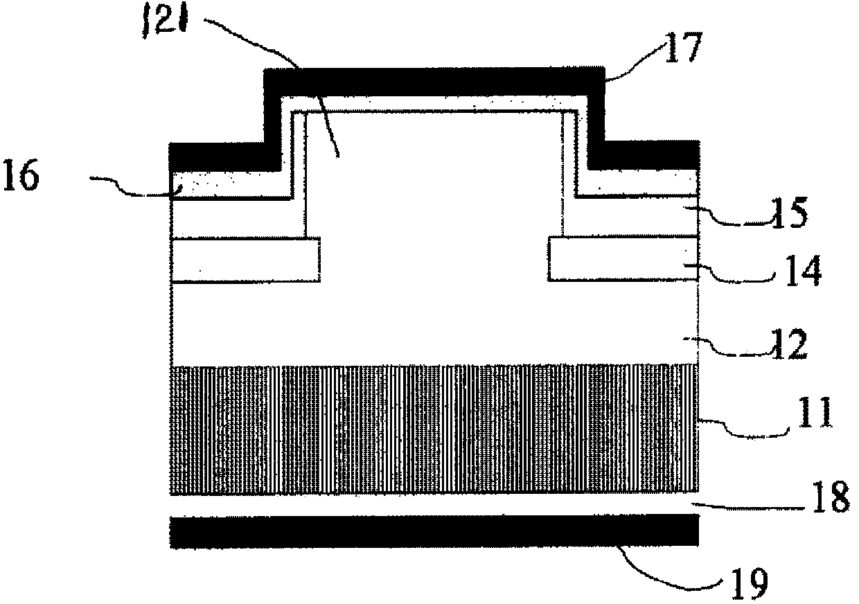
[0030] see figure 1 , the present invention provides a trench type MOS barrier Schottky diode, comprising:
[0031] A substrate 11, the material of the substrate 11 is N-type or P-type 4H or 6H silicon carbide, the material of the substrate 11 is N-type or P-type 4H or 6H silicon carbide, and the thickness of the substrate 11 is 1 μm -500 μm, the surface area of the substrate 11 is 1 μm 2 -2000cm 2 ;
[0032] An epitaxial film 12, which is made on the substrate 11, has a boss 121 in the middle of the epitaxial film 12, the sidewall of the boss 121 is a plane, and the material of the epitaxial film 12 is N-type or P-type 4H or 6H silicon carbide , the thickness of the epitaxial film 12 is 1 μm-200 μm, and the surface area of the substrate 11 is 1 μm 2 -2000cm 2 ;
[0033] A guard ring 14, which is made around the boss 121 of the epitaxial film 12, and is located on the plane around the boss 121. The boss 121 is an interdigitated, parallel strip, circular or square tab...
PUM
| Property | Measurement | Unit |
|---|---|---|
| Thickness | aaaaa | aaaaa |
| Height | aaaaa | aaaaa |
| Depth | aaaaa | aaaaa |
Abstract
Description
Claims
Application Information