Highly voltage-withstanding schottky chip

A high withstand voltage, chip technology, applied in the direction of electrical components, circuits, semiconductor devices, etc., can solve the problems of low reverse withstand voltage of Schottky chips, cannot meet high withstand voltage or reduce forward voltage drop, etc., to achieve improved efficiency effect

Inactive Publication Date: 2013-03-27
淄博美林电子有限公司
View PDF3 Cites 2 Cited by
  • Summary
  • Abstract
  • Description
  • Claims
  • Application Information

AI Technical Summary

Problems solved by technology

[0002] For traditional Schottky chips, the thickness of the trench silicon oxide layer outside the polysilicon is consistent, such as figure 2 As shown, electrical breakdown is prone to occur at the corner of the bottom of the trench, so the reverse withstand voltage of the Schottky chip is low, which cannot meet the requirements of high withstand voltage or reduce forward voltage drop

Method used


Image

  • Highly voltage-withstanding schottky chip
  • Highly voltage-withstanding schottky chip

Examples


Embodiment Construction

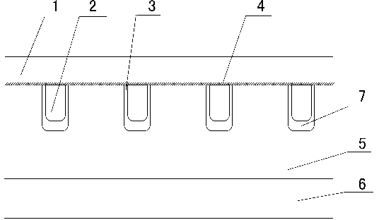
[0012] figure 1 It is the best embodiment of the present invention. Attached below figure 1 A high withstand voltage Schottky chip of the present invention is further described.

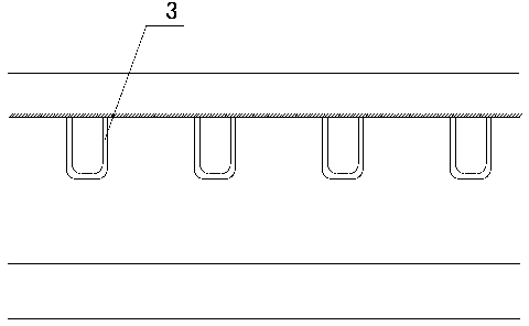
[0013] This high withstand voltage Schottky chip consists of top metal layer 1, polysilicon 2, side silicon oxide layer 3, Schottky interface 4, N-type epitaxial layer N-EPI5, N-type substrate N + Substrate6 and bottom silicon oxide layer 7. N type substrate N + Substrate6 is heavily doped N-type substrate. From bottom to top: N-type substrate N + Substrate6, N-type epitaxial layer N-EPI 5 , bottom silicon oxide layer 7, polysilicon 2, side silicon oxide layer 3, Schottky interface 4 and top metal layer 1, silicon oxide layer outside polysilicon 2 bottom silicon oxide layer 7 The thickness is greater than the thickness of the silicon oxide layer 3 at the edge. The thickness of the bottom silicon oxide layer 7 is 2-5 times of the thickness of the side silicon oxide layer 3 .

[0014] For ex...


PUM


Abstract

The invention discloses a highly voltage-withstanding schottky chip and belongs to the technical field of semiconductor device production. The chip comprises a top metal layer (1), a schottky interface (4) under the top metal layer (1), polysilicon (2) closely attached to the underside of the schottky interface (4), a silicon oxide layer outside the polysilicon (2), an N-type epitaxial layer N-EPI (5) and an N-type substrate N+Substrate (6) on the lower portion. The chip is characterized in that the thickness of a bottom silicon oxide layer (7) of the silicon oxide layer outside the polysilicon (2) is larger than that of a side silicon oxide layer (3). Due to the fact that the bottom thickness of the silicon oxide is larger than that in the prior art, the reverse voltage of an electric field at a bending position at the bottom of a groove is untwined, so that the reverse voltage withstanding of a product can be improved by 15%-30%.

Description

technical field [0001] A high withstand voltage Schottky chip belongs to the technical field of semiconductor device manufacturing. It specifically relates to a high withstand voltage Schottky N-channel Schottky chip. Background technique [0002] For traditional Schottky chips, the thickness of the trench silicon oxide layer outside the polysilicon is consistent, such as figure 2 As shown, electrical breakdown is prone to occur at the corner of the bottom of the trench, so the reverse withstand voltage of the Schottky chip is low, which cannot meet the requirements of high withstand voltage or reduce forward voltage drop. Contents of the invention [0003] The technical problem to be solved by the present invention is to overcome the deficiencies of the prior art and provide a high withstand voltage Schottky chip that can increase the reverse withstand voltage of the Schottky chip or reduce the forward voltage drop. [0004] The technical solution adopted by the present...

Claims


Application Information

Patent Timeline
Patent Type & Authority Applications(China)
IPC IPC(8): H01L29/06
Inventor 关仕汉吕新立
Owner 淄博美林电子有限公司
Why Eureka
Try Eureka