Supercharge Your Innovation With Domain-Expert AI Agents!

FPGA (Field-Programmable Gate Array)-based CIS (Contact Image Sensor) image acquisition system and acquisition method thereof

An image acquisition system and acquisition module technology, which is applied in image communication, components of TV systems, and optical devices, etc., can solve problems such as inability to adapt to manual detection, and achieve the effect of improving the pass rate.

Inactive Publication Date: 2012-08-01
GUANGDONG ZHENGYE TECH +1
View PDF2 Cites 10 Cited by
  • Summary
  • Abstract
  • Description
  • Claims
  • Application Information

AI Technical Summary

Problems solved by technology

[0003] The development of the PCB industry has made it impossible to adapt to manual inspection; through the acquisition of PCB images by CIS, through software analysis and processing, defects in the PCB board can be easily detected and the competitiveness of PCB manufacturers has been improved; but how to better Using FPGA for CIS image acquisition, the acquisition system is becoming more and more accurate

Method used


Image

  • FPGA (Field-Programmable Gate Array)-based CIS (Contact Image Sensor) image acquisition system and acquisition method thereof
  • FPGA (Field-Programmable Gate Array)-based CIS (Contact Image Sensor) image acquisition system and acquisition method thereof
  • FPGA (Field-Programmable Gate Array)-based CIS (Contact Image Sensor) image acquisition system and acquisition method thereof

Examples


Embodiment Construction

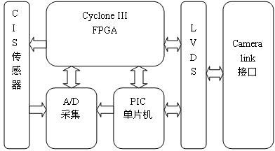
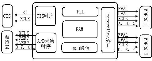
[0031] The gist of the present invention is to overcome the deficiencies in the prior art, and provide a CIS image acquisition system based on FPGA and its acquisition method. The system is composed of FPGA, single-chip microcomputer, AD converter, and LVDS chip. The output image is collected by AD, converted into a digital signal, preprocessed by FPGA, and stored in internal RAM. According to the cameralink data format, the data is output to the cameralink interface in the form of differential through the LVDS chip.

[0032] The FPGA provides the working timing for the CIS sensor, and the analog signal output by the CIS is collected by AD, and after preprocessing such as FPGA denoising and binarization, it is stored in the internal RAM of the FPGA. After obtaining the user-set parameters of the single-chip microcomputer according to the FPGA, select the output image type; the output image is sent to the cameralink interface in a differential manner through the LVDS chip, and i...


PUM


Abstract

The invention discloses an FPGA (Field-Programmable Gate Array)-based CIS (Contact Image Sensor) image acquisition system and an acquisition method thereof. The acquisition system comprises a CIS and further comprises an AD acquisition module, an FPGA data processing module, an LVDS (Low Voltage Differential Signaling) conversion module, a single chip control module and a cameralink interface, wherein the AD acquisition module is connected with an output end of the CIS; the FPGA data processing module is in both-way connection with the AD acquisition module; the LVDS conversion module and the single chip control module are in both-way connection with the FPGA data processing module; the cameralink interface is in both-way connection with the LVDS conversion module; the single chip control module is in both-way connection with the LVDS conversion module; the output end of the single chip control module is connected with an input end of the AD acquisition module; a PIC single chip is served as the single chip of the single chip control module; and the output end of the FPGA data processing module is connected with the CIS. The acquisition system provided by the invention is capable of accurately acquiring and detecting a CIS image, detecting the defects existing in a PCB (Printed Circuit Board) and increasing the yield of the PCB.

Description

technical field [0001] The present invention relates to a linear array contact image acquisition system used in hole inspection machines or other fields of the PCB industry, in particular to a CIS (Contact Image Sensor, contact image sensor) image acquisition system and acquisition method thereof. Background technique [0002] The contact image sensor (CIS) was developed in the early 1990s. Due to its compact structure, no complex optical lens components, small size, light weight, good shock resistance, and fast response, it has gradually replaced part of the CCD market. It is widely used in faxing, scanning, banknote bill recognition, and cursor reading. At the same time, the application of CIS in the PCB industry reduces the volume of testing instruments and increases stability and cost performance. [0003] The development of the PCB industry has made it impossible to adapt to manual inspection; through the acquisition of PCB images by CIS, through software analysis and ...

Claims


Application Information

Patent Timeline
IPC IPC(8): H04N5/369H04N1/031G01N21/956G01B11/08
Inventor 刘敏梁波梅领亮徐地华
Owner GUANGDONG ZHENGYE TECH
Features
  • R&D
  • Intellectual Property
  • Life Sciences
  • Materials
  • Tech Scout
  • Unparalleled Data Quality
  • Higher Quality Content
  • 60% Fewer Hallucinations
Learn More