Method for manufacturing solder mask of unit plate by using electrostatic spray coating machine

A technology of electrostatic spraying and unit board, which is applied in the direction of coating non-metallic protective layer and secondary treatment of printed circuit, etc., which can solve the problems of easy scratching of the board surface, easy plugging of ink holes, troublesome operation, etc., to avoid material waste, Ease of operation and improvement of production efficiency

Inactive Publication Date: 2014-09-03
SHENZHEN SUNTAK MULTILAYER PCB
View PDF3 Cites 0 Cited by
  • Summary
  • Abstract
  • Description
  • Claims
  • Application Information

AI Technical Summary

Problems solved by technology

[0004] In view of this, the purpose of the present invention is to provide a method for making the solder resist layer of the unit board by an electrostatic spraying machine, so as to solve the problems of troublesome operation and high cost, easy plugging of ink, etc. The surface of the board is easy to scratch and not oily and other quality problems

Method used


Image

  • Method for manufacturing solder mask of unit plate by using electrostatic spray coating machine
  • Method for manufacturing solder mask of unit plate by using electrostatic spray coating machine
  • Method for manufacturing solder mask of unit plate by using electrostatic spray coating machine

Examples


Embodiment Construction

[0025] In order to illustrate the idea and purpose of the present invention, the present invention will be further described below in conjunction with the accompanying drawings and specific embodiments.

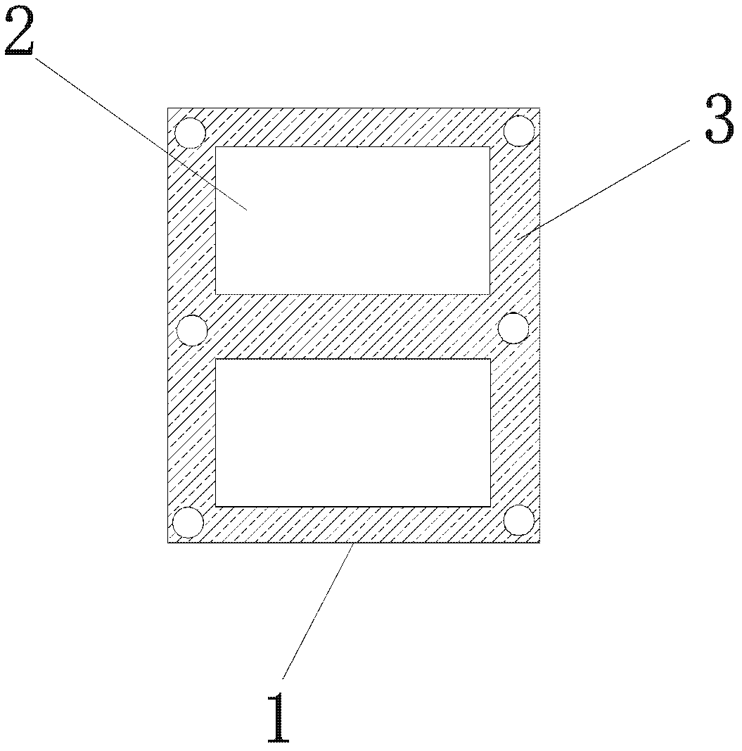
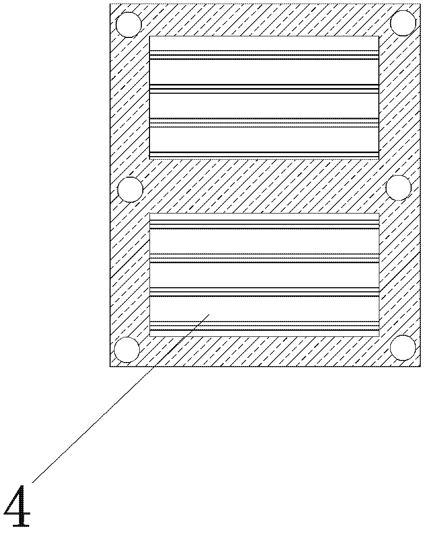
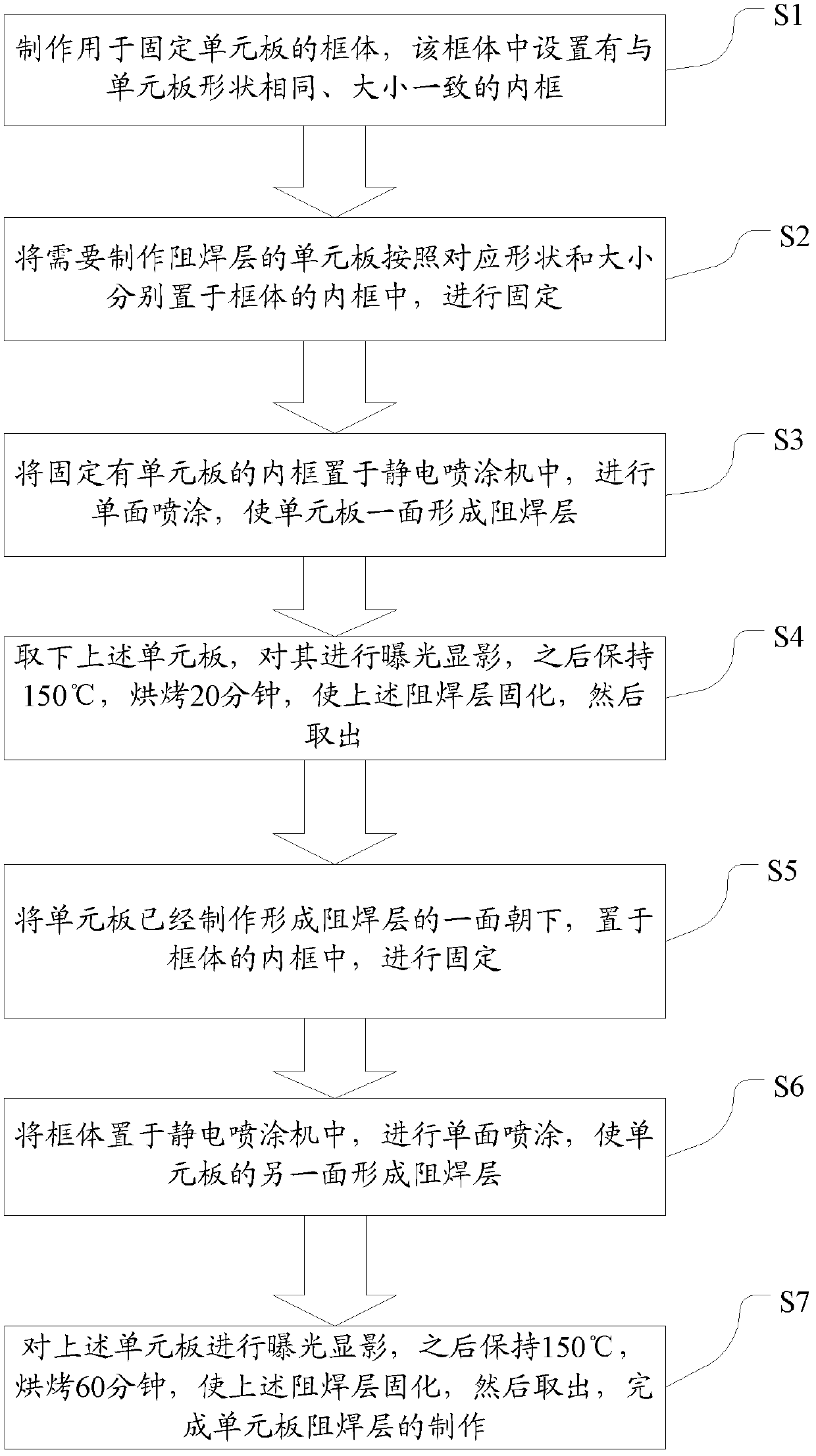
[0026] See figure 1 , figure 2 , image 3 as shown, figure 1 It is a structural schematic diagram of the framework of the present invention; figure 2 It is a structural schematic diagram of the fixed unit plate in the frame of the present invention; image 3 It is a process flow diagram of the present invention. The invention provides a method for making a solder resist layer of a unit board by an electrostatic spraying machine, which is mainly used to solve the troublesome operation, high cost, high requirements for operators and easy operation of solder resist ink printing using a screen printing screen. Cause the problems of ink rubbing and ink plugging on the surface of the unit board.

[0027] Wherein the method for making the solder resist layer of the unit boar...


PUM


Abstract

The invention discloses a method for manufacturing a solder mask of a unit plate by using an electrostatic spray coating machine. A frame is manufactured, an inner frame with same shape and size of the unit plate is arranged on the frame and is used for fixing the unit plate, and a clamping force to the frame is formed by the electrostatic spray coating machine, so that the problems of easily scratched plate surface and ink tightness caused by the direct contact between a clamp and the unit plate are avoided. Compared with the prior art, the method provided by the invention has the advantages: printing ink cannot enter into a hole because the printing ink of the electrostatic spray coating machine has negative electricity and achieves an electrostatic shielding effect while acting on the hole, the production quality is ensured, the operation in such a manner is convenient, the complex operations, such as manual net filling, 'hand pushing' silk printing, are omitted, and the production efficiency is increased. The frame is used for preventing labor from directly contacting the surface of the unit plate, so that the quality of product is ensured and the unnecessary material waste is avoided.

Description

Technical field: [0001] The invention belongs to the technical field of printed circuit board production, and specifically relates to a method for producing a solder resist layer of a unit board by an electrostatic spraying machine. Process improvements for rework. Background technique: [0002] When making circuit boards, one or more unit boards are first assembled into a large board for each process, and finally the invalid board edge of the large board is milled off in the "forming" process to form the required unit board. Usually, the invalid board edge of the large board is designed with board edge graphics required by various processes, and these graphics can be used to complete the positioning work of exposure, drilling, pressing and solder mask processes. When it is found that there is a solder mask problem on the unit board after molding, it is necessary to rework the solder mask layer. [0003] At present, for the rework of the unit board due to the solder resist...

Claims


Application Information

Patent Timeline
Patent Type & Authority Patents(China)
IPC IPC(8): H05K3/28
Inventor 朱拓宋建远鲁惠魏秀云梁水娇
Owner SHENZHEN SUNTAK MULTILAYER PCB
Why Eureka
Try Eureka