Thin film transistor (TFT) array substrate, manufacture method thereof and display device

The technology of an array substrate and a manufacturing method is applied in the field of a TFT array substrate and its manufacturing method and a display device, which can solve the problems that the light transmittance cannot be significantly improved, and achieve the effect of improving the light transmittance

Active Publication Date: 2012-08-08
BOE TECH GRP CO LTD
View PDF4 Cites 19 Cited by
  • Summary
  • Abstract
  • Description
  • Claims
  • Application Information

AI Technical Summary

Problems solved by technology

However, the effect of the improved TFT substrate on preventing the reverse rotation domains and disclination lines of the liquid crystal generated at the corners of the electrode slit is not obvious, and the light transmittance in this area cannot be significantly improved.

Method used


Image

  • Thin film transistor (TFT) array substrate, manufacture method thereof and display device
  • Thin film transistor (TFT) array substrate, manufacture method thereof and display device
  • Thin film transistor (TFT) array substrate, manufacture method thereof and display device

Examples


Embodiment Construction

[0026] The following will clearly and completely describe the technical solutions in the embodiments of the present invention with reference to the accompanying drawings in the embodiments of the present invention. Obviously, the described embodiments are only some, not all, embodiments of the present invention. Based on the embodiments of the present invention, all other embodiments obtained by persons of ordinary skill in the art without making creative efforts belong to the protection scope of the present invention.

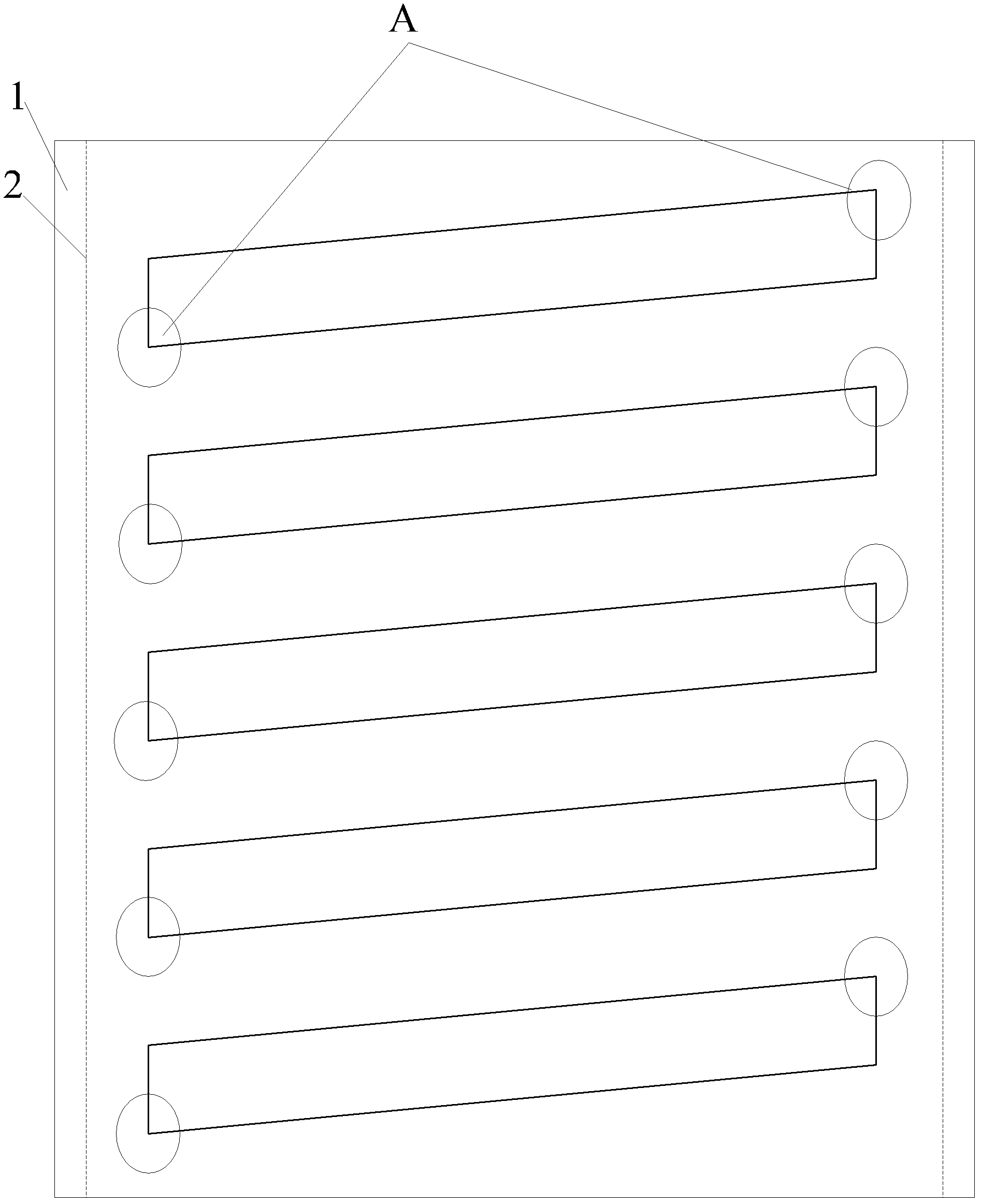
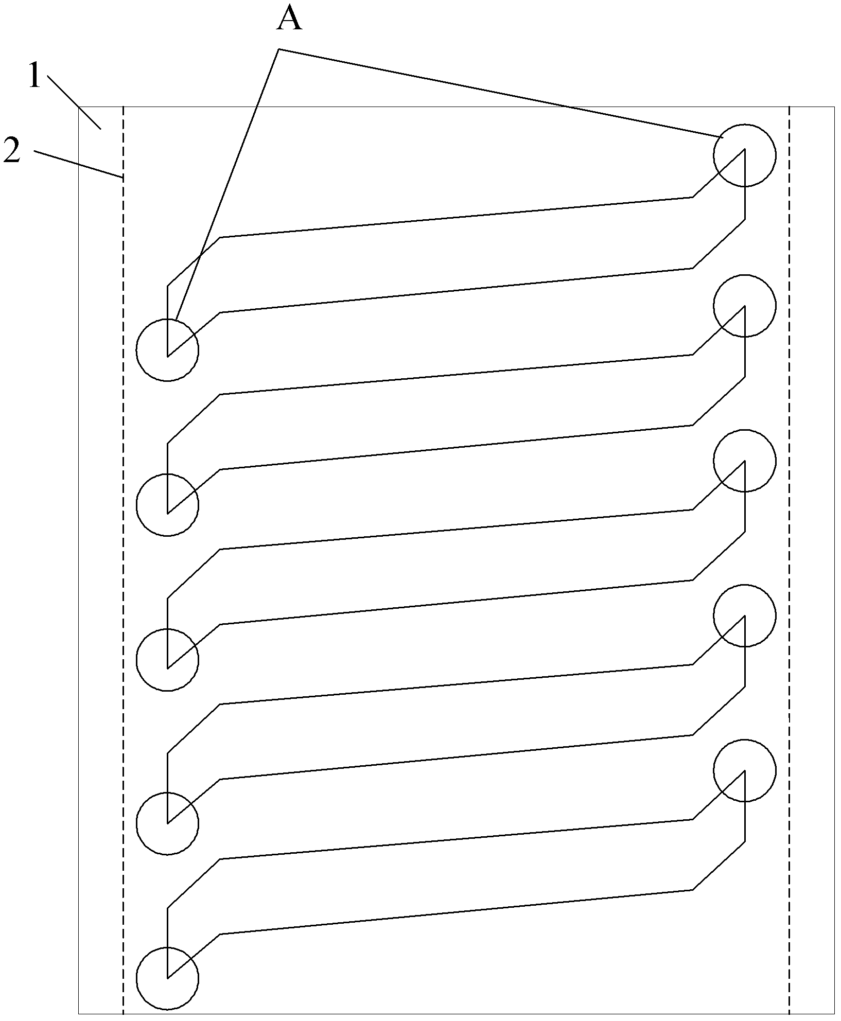
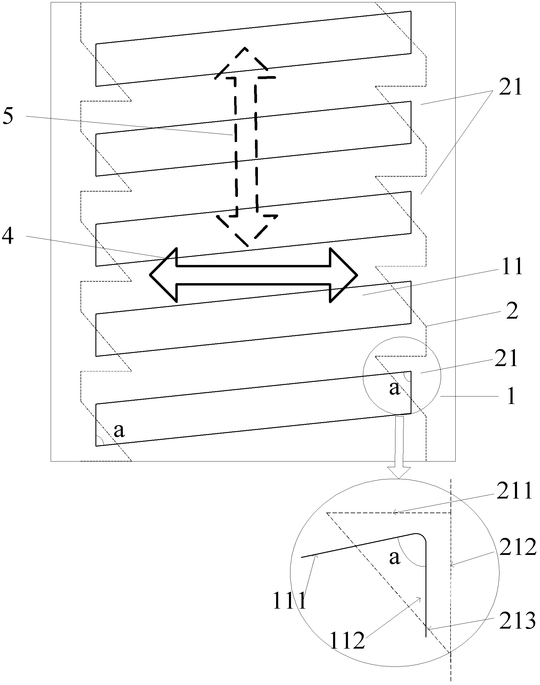
[0027] The TFT array substrate of the ADS mode that the embodiment of the present invention provides, such as image 3 As shown, it includes: an upper layer electrode 1 with a slit 11 and a whole lower layer electrode 2 . Wherein, the slit 11 of the upper electrode 1 is a parallelogram and includes at least one pair of angles ∠α less than or equal to 90 degrees. In this embodiment, the top of ∠α may be a rounded corner. The lower electrode 2 has a defect area...


PUM


Abstract

The invention provides a thin film transistor (TFT) array substrate, a manufacture method thereof and a display device, which relate to the field of display device manufacture and prevent an electrode slit corner from generating a liquid crystal contrarotation domain and a disclination line so as improve light transmitting rate of the area. The method includes that by changing the shape of a lower-layer electrode, and the slit corner of an upper-layer electrode and the lower-layer electrode do not have corresponding overlapping in the vertical direction so that electric field strength of the area is weakened. An embodiment of the TFT array substrate, the manufacture method and the display device is applied to manufacture of the TFT array substrate.

Description

technical field [0001] The invention relates to the field of display device manufacturing, in particular to a TFT array substrate, a manufacturing method thereof, and a display device. Background technique [0002] Thin Film Transistor Liquid Crystal Display (TFT-LCD for short) has the characteristics of small size, low power consumption, and no radiation, and occupies a dominant position in the current flat panel display market. [0003] ADSDS (ADvanced Super Dimension Switch), referred to as ADS, is the advanced super-dimensional field switching technology. The electric field generated by the edge of the slit electrode in the same plane and the electric field generated between the slit electrode layer and the plate electrode layer form a multi-dimensional electric field. All oriented liquid crystal molecules between the slit electrodes in the liquid crystal cell and directly above the electrodes can rotate, thereby improving the working efficiency of the liquid crystal and...

Claims


Application Information

Patent Timeline
Patent Type & Authority Applications(China)
IPC IPC(8): G02F1/1343G02F1/1362G02F1/1368H01L27/02H01L21/77
CPCG02F1/133707G02F1/1343G02F1/134363G02F1/13373G02F1/134318G02F1/134372G02F1/136277
Inventor 铃木照晃
Owner BOE TECH GRP CO LTD
Why Eureka
Try Eureka