

Manufacturing method of component baseplate
A component substrate and manufacturing method technology, which is applied in semiconductor/solid-state device manufacturing, electrical components, circuits, etc., can solve the problems of laser regulation ability affecting yield, production capacity, and production cost increase
- Summary
- Abstract
- Description
- Claims
- Application Information
AI Technical Summary
Problems solved by technology
Method used
Image

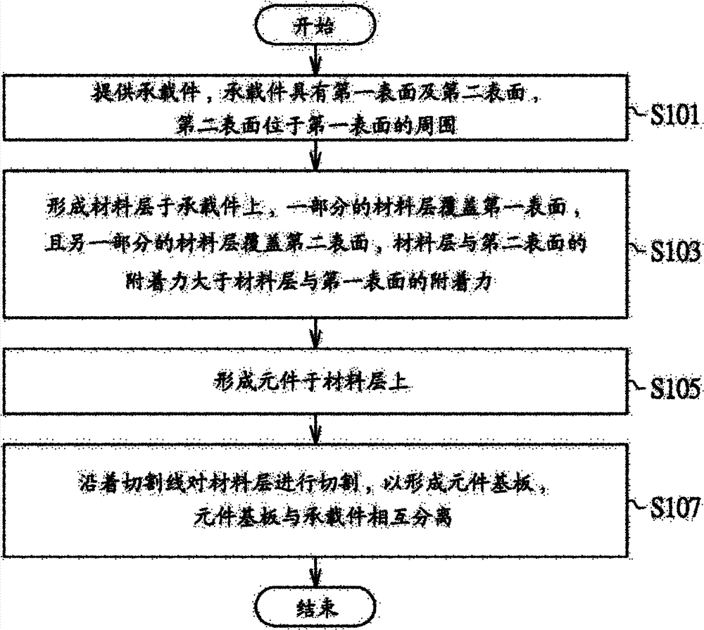
Examples
no. 1 example
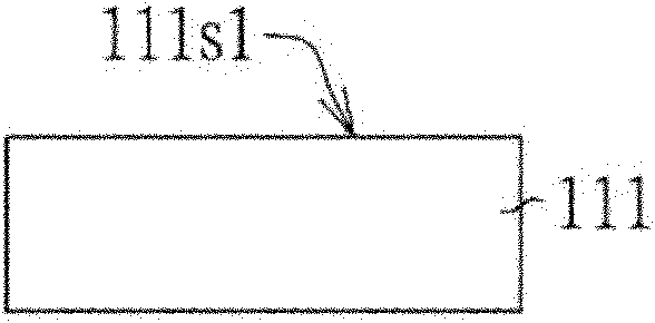
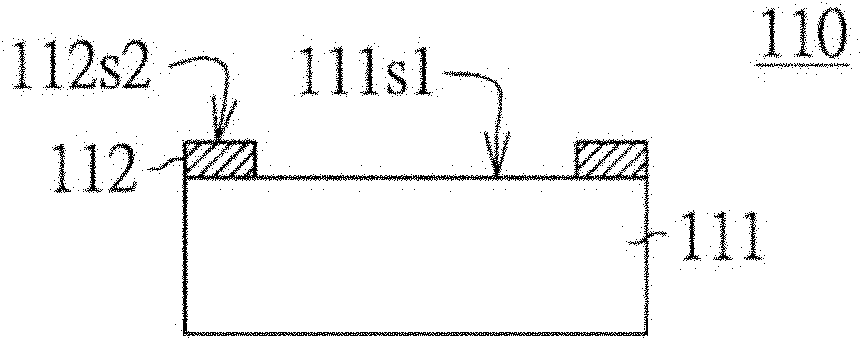
[0044] Please refer to Figure 2A ~ Figure 2E , which shows a schematic flow chart of a first manufacturing method of an element substrate according to a first embodiment of the present invention. Figure 2A and Figure 2B corresponds to figure 1in step S101, and Figure 2C ~ Figure 2E corresponding to figure 1 Step S103 to step S107 in. It will be described in detail below.
[0045] pass Figure 2A and Figure 2B The carrier 110 provided in the process has a first surface 111s1 and a second surface 112s2, and the second surface 112s2 is located around the first surface 111s1.
[0046] exist Figure 2A In this example, a carrier board 111 is provided, and the carrier board 111 has a first surface 111s1.
[0047] Next, at Figure 2B In the process, the patterned release structure 112 is formed on the first surface 111s1 of the carrier 111 to form the carrier 110 . The release structure 112 has a second surface 112s2. The release structure 112 here can be, for exampl...
no. 2 example
[0059] Please refer to Figure 4A ~ Figure 4E , which is a schematic flowchart of a method for manufacturing an element substrate according to a second embodiment of the present invention. Compared with the second method of manufacturing the element substrate 100 of the first embodiment, the method of manufacturing the element substrate 200 of this embodiment roughens the surface in different ways to change the adhesion of the surface. Figure 4A and Figure 4B corresponds to figure 1 in step S101, and Figure 4C ~ Figure 4E corresponding to figure 1 Step S103 to step S107 in. It will be described in detail below.
[0060] pass Figure 4A and Figure 4B The carrier 310 provided in the process has a first surface 311s1 and a second surface 311s2, and the second surface 311s2 is located around the first surface 311s1.
[0061] exist Figure 4A In this example, a carrier board 311 is provided, and the carrier board 311 has a first surface 311s1.
[0062] Next, at Figu...
no. 3 example
[0067] Please refer to Figure 5A ~ Figure 5E , which shows a schematic flowchart of a method for manufacturing an element substrate according to a third embodiment of the present invention. Compared with the first manufacturing method of the element substrate 100 in the first embodiment, the arrangement position and material of the release structure 412 in this embodiment are different. Figure 5A and Figure 5B corresponds to figure 1 in step S101, and Figure 5C ~ Figure 5E corresponding to figure 1 Step S103 to step S107 in. It will be described in detail below.
[0068] pass Figure 5A and Figure 5B The carrier 410 provided in the process has a first surface 412s1 and a second surface 411s2, and the second surface 411s2 is located around the first surface 412s1.
[0069] like Figure 5A As shown, a carrier 411 is provided having a second surface 411s2.
[0070] Next, if Figure 5BAs shown, a patterned release structure 412 is formed on the second surface 411s2...
PUM
 Abstract
Description
Claims
Application Information