
LED (light-emitting diode) chip carrier positioning and absorbing device

A technology of LED chips and adsorption devices, which is applied in semiconductor/solid-state device manufacturing, semiconductor/solid-state device testing/measurement, electrical components, etc., and can solve processing delays, uneven negative pressure absorption, and surface wrinkling of crystal gardens, etc. problems, to facilitate construction operations, avoid surface wrinkling, and reduce production costs

Inactive Publication Date: 2012-08-15
PUTIAN UNIV
View PDF5 Cites 22 Cited by
  • Summary
  • Abstract
  • Description
  • Claims
  • Application Information

AI Technical Summary

Problems solved by technology

Because the existing suction cups generally have the problem of uneven suction and payment of various parts, it often causes wrinkles on the surface of the wafer, which affects the detection and positioning of LED chips
In previous applications, due to the wrinkling of the crystal garden, the positioning of the LED chip was inaccurate, and in severe cases, the wafer garden was damaged, and the direct loss was more than 10,000 yuan at a time. More than 100,000 yuan
[0003] In addition, because the existing suction cup cannot rotate the angle, it also affects the flexibility of LED chip detection

Method used


Image

  • LED (light-emitting diode) chip carrier positioning and absorbing device
  • LED (light-emitting diode) chip carrier positioning and absorbing device
  • LED (light-emitting diode) chip carrier positioning and absorbing device

Examples


Embodiment Construction

[0015] The content of the present invention will be described in detail below in conjunction with the accompanying drawings and embodiments of the description:

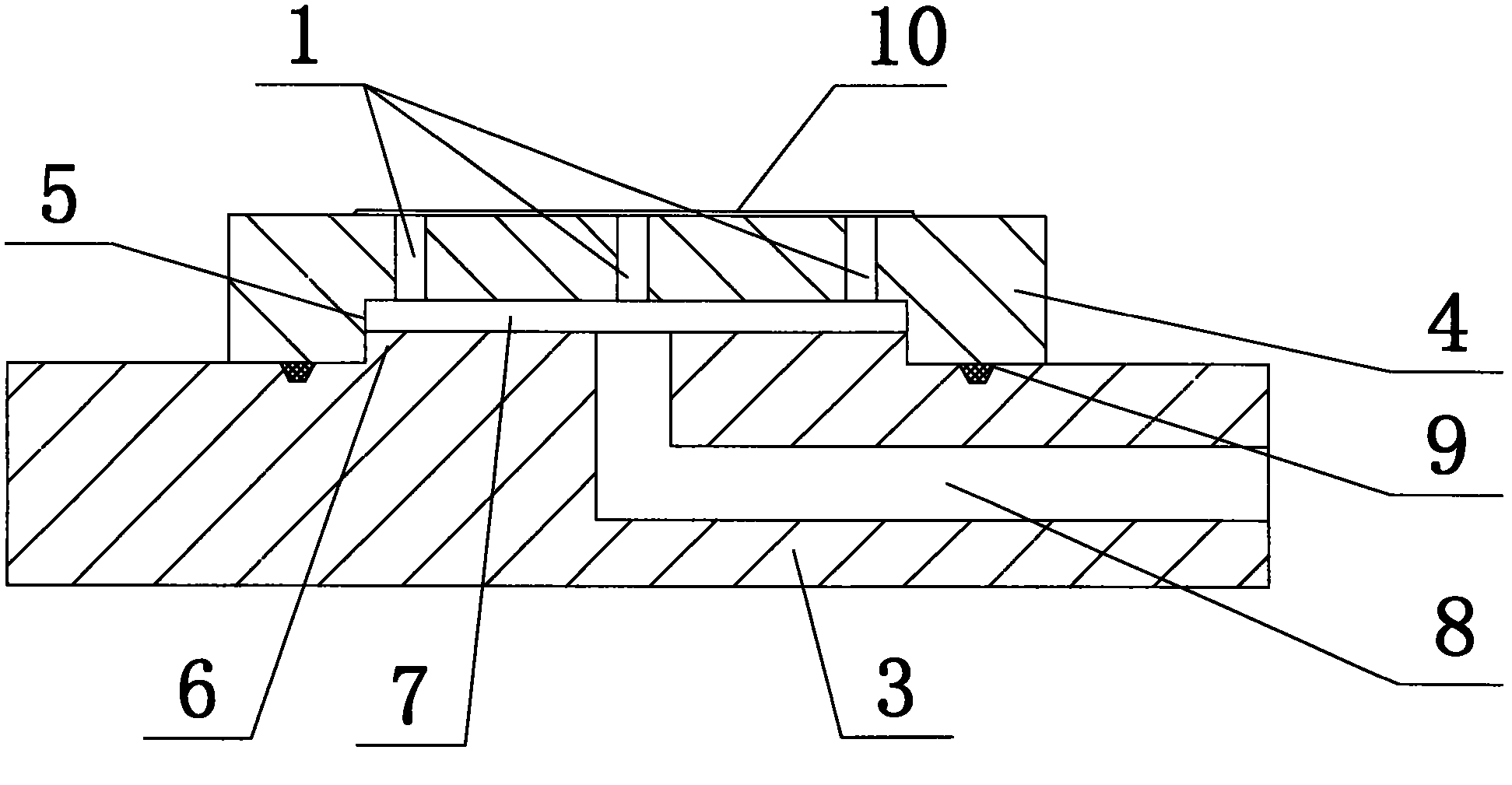
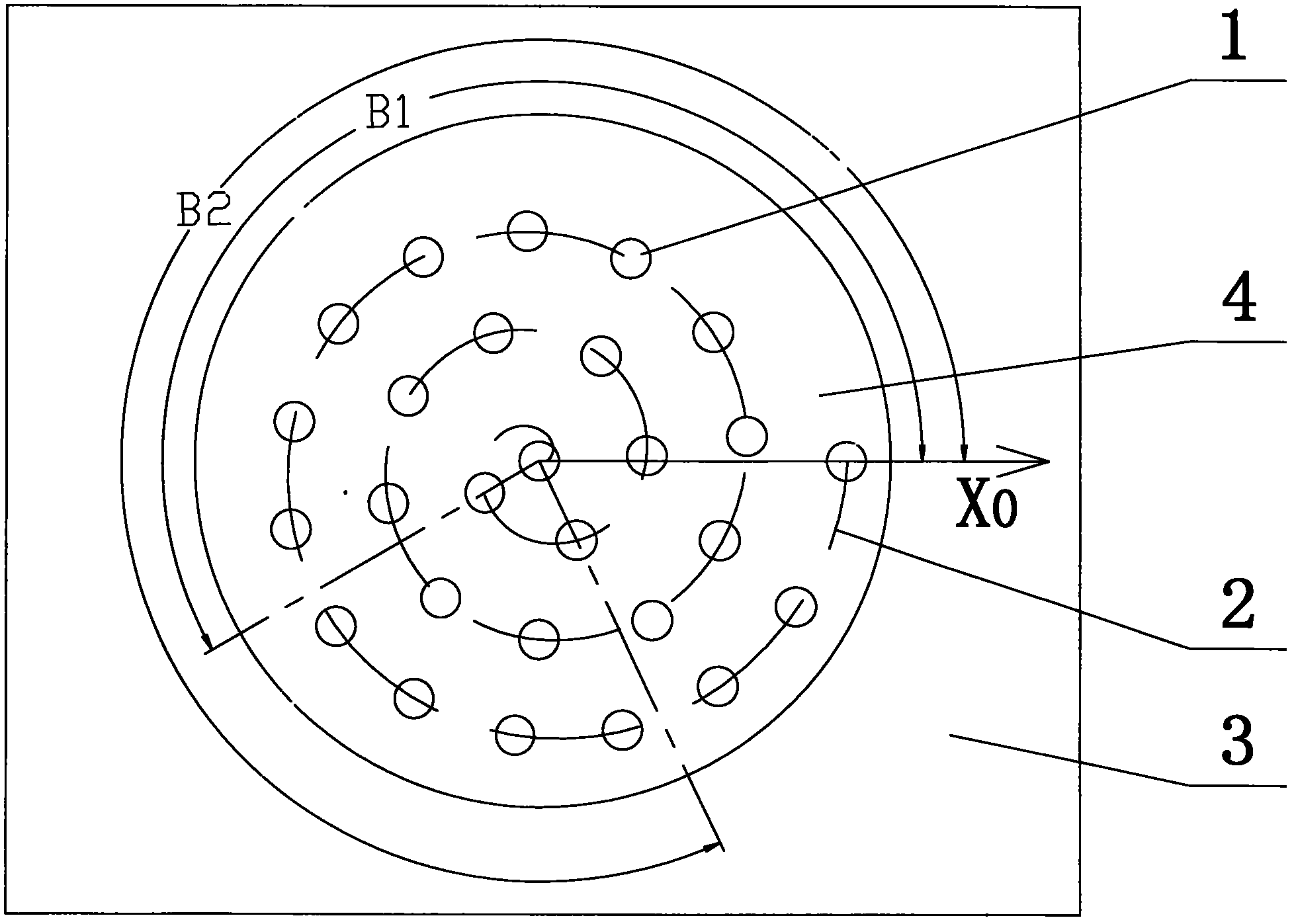
[0016] Such as Figure 1-Figure 2 Shown is a schematic structural diagram of an embodiment of an LED chip carrier positioning and adsorption device provided by the present invention, which is characterized in that: it includes an adsorption table with an adsorption plane; the adsorption plane is provided with a plurality of adsorption holes 1; An air extraction channel is arranged in the adsorption table body, the inlet end of the air extraction channel is connected with each adsorption hole 1, and the outlet end of the air extraction channel is connected with a vacuum device; The center of the spiral is the starting point and arranged in sequence along the extension direction of the Archimedes spiral 2. The adsorption hole 1 located at the spiral center of the Archimedes spiral 2 is the central hole. Except for the c...


PUM


Abstract

The invention relates to an LED (light-emitting diode) chip carrier positioning and absorbing device which comprises an absorbing platform with an absorbing plane; the absorbing plane is provided with a plurality of absorbing holes; an absorbing platform body is internally provided with an air pumping channel, the inlet end of the air pumping channel is communicated with each absorbing hole and the outlet end of the air pumping channel is connected with a vacuumizing device; each absorbing hole is sequentially distributed and arrayed by taking the spiral center of the Archimedes spiral line as a starting point along the extending direction of the Archimedes spiral line; the absorbing hole positioned at the spiral center of the Archimedes spiral line is a central hole, except for the central hole, an included angle of the connecting lines of the hole core of each absorbing hole and the spiral center of the Archimedes spiral line relative to a starting coordinate axis X0 meets the following relationship Bn=n<1 / 2> *B1. According to the invention, an LED chip carrier can be uniformly absorbed and positioned on the absorbing plane of the absorbing platform, the phenomenon of surface wrinkling generated when the LED chip carrier is absorbed is prevented, and the accuracy of the detection and positioning of an LED chip is improved.

Description

technical field [0001] The invention relates to an LED chip carrier positioning and adsorption device, which is mainly used in the technical field of LED chip detection, and is a positioning component of equipment such as a detection machine, a sorting machine, and a crystal bonding machine. Background technique [0002] The size of LED chips is only about 0.2×0.2mm, and they are usually arranged in a square array on a 2-inch crystal garden. There are about 40,000 LED chips carried on a crystal garden. During detection and sorting, it is necessary to fix the crystal garden on the suction cup in order to detect the chips. Because the existing suction cup generally has the problem of uneven suction and payment of various parts, it often causes wrinkles on the surface of the wafer, which affects the detection and positioning of the LED chip. In previous applications, due to the wrinkling of the crystal garden, the positioning of the LED chip was inaccurate, and in severe cases...

Claims


Application Information

Patent Timeline
IPC IPC(8): H01L21/683H01L21/66
Inventor 吴晓
Owner PUTIAN UNIV
Learn More