
PCB (printed circuit board)

A PCB board, positioning hole technology, applied in the direction of printed circuit components, etc., can solve the problems of easy sliding and inaccurate positioning, and achieve the effect of increasing the pulling force, accurate positioning, and avoiding the dislocation of the overall skateboard.

Inactive Publication Date: 2012-08-15
SHENNAN CIRCUITS
View PDF2 Cites 4 Cited by
  • Summary
  • Abstract
  • Description
  • Claims
  • Application Information

AI Technical Summary

Problems solved by technology

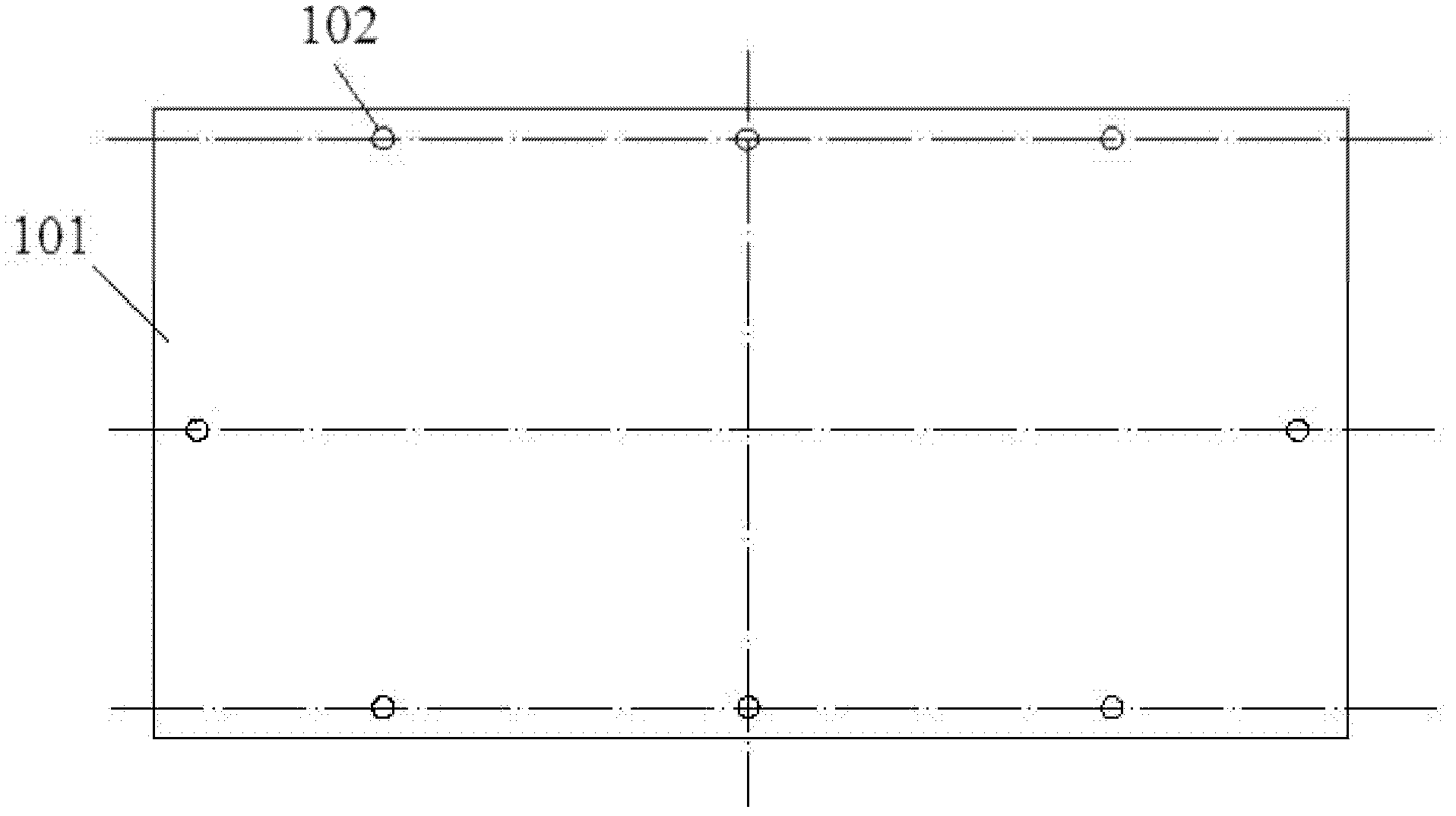
[0003] The defect of the existing linear frame positioning method is that the longitudinal and horizontal pressing positioning holes are located on a straight line, which is prone to slippage during pressing positioning, and the positioning frame formed by the longitudinal and horizontal pressing positioning holes is composed of a rectangular shape. Becomes a parallelogram with hypotenuses, resulting in an overall slide between the backplanes and inaccurate positioning

Method used


Image

  • PCB (printed circuit board)
  • PCB (printed circuit board)
  • PCB (printed circuit board)

Examples


Embodiment 1

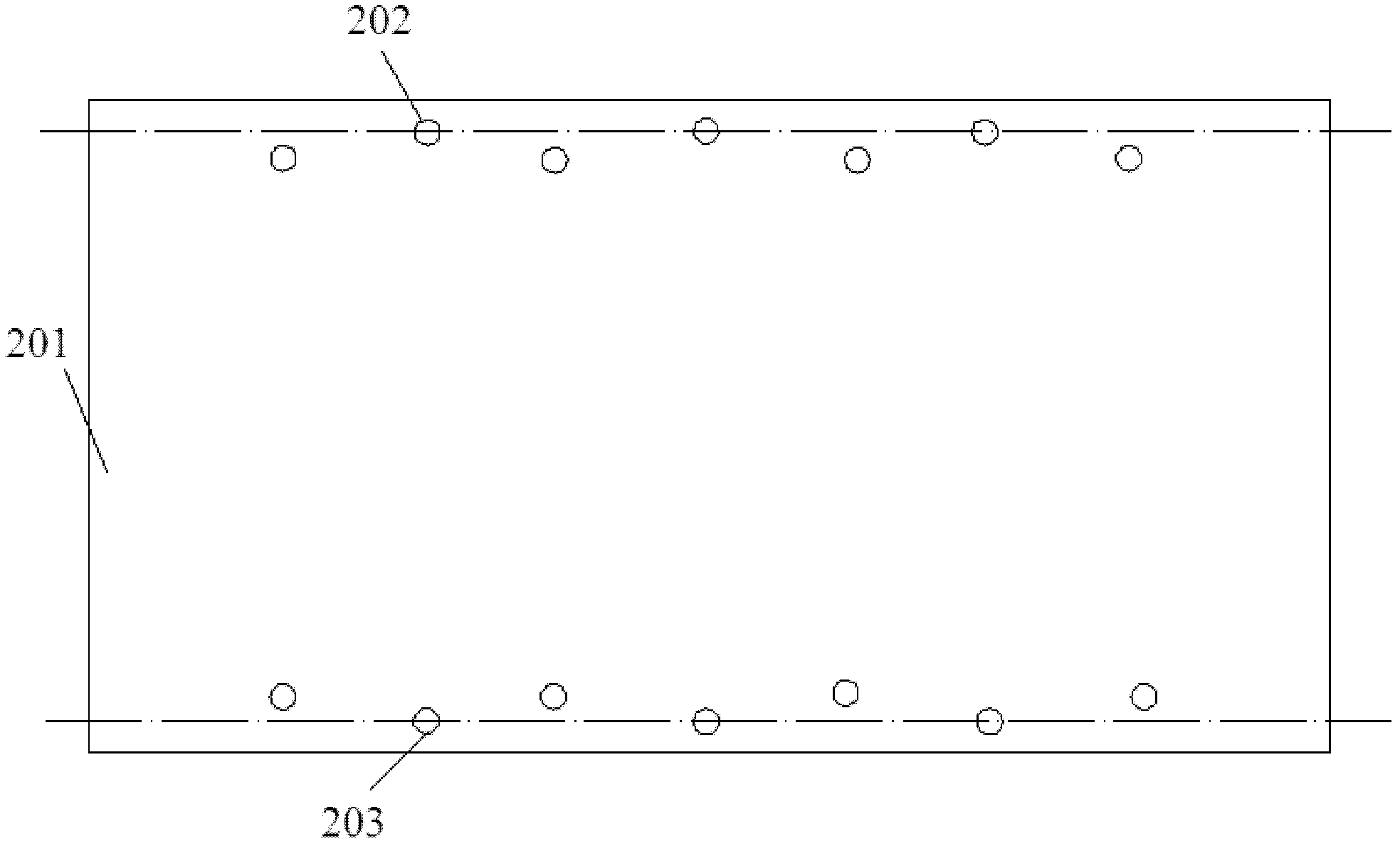
[0021] like figure 2 As shown, a PCB board 201 includes: the first end of the PCB board 201 is provided with a first press-fit positioning hole 202, and the second end of the PCB board is provided with a second press-fit positioning hole 203. The first press-fit positioning holes 202 are arranged in waves in the transverse direction, and the first end is opposite to the second end. The first press-fit positioning holes 202 arranged in a wavy pattern enable the PCB board to be pulled obliquely when it is press-fitted and positioned, and will not cause the overall slide of the PCB to be dislocated.

Embodiment 2

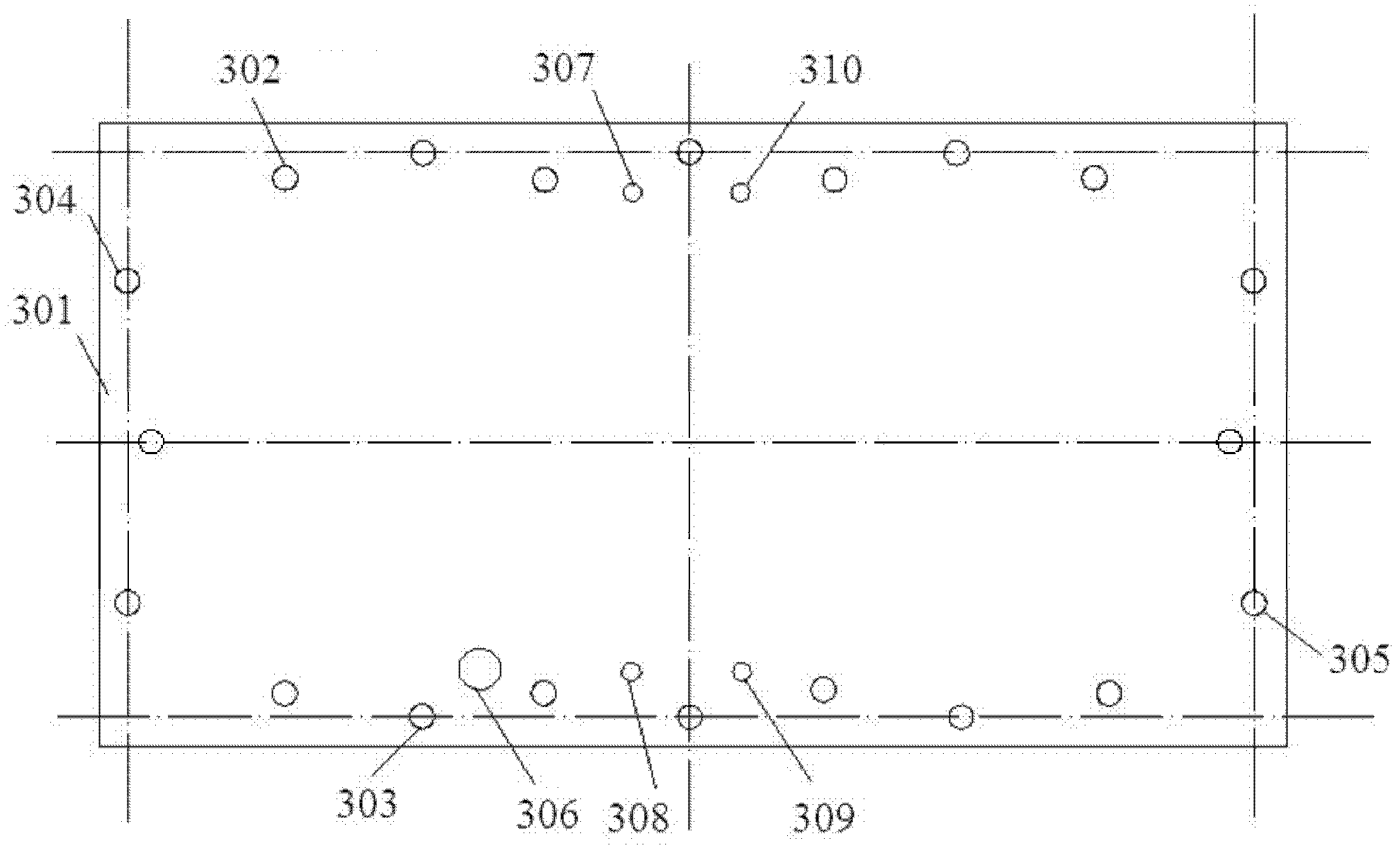
[0023] like image 3 As shown, a PCB board 301, the first end of the PCB board 301 is provided with a first pressing positioning hole 302, the second end of the PCB board is provided with a second pressing positioning hole 303, the first The press-fit positioning holes 302 are arranged in waves in the transverse direction, the second press-fit positioning holes 303 are arranged in waves in the transverse direction, and the first end is opposite to the second end. The press-fit positioning holes at the second end of the PCB board are arranged in waves, so that when the PCB board is press-fit and positioned, the oblique pulling force is greater, and the overall slide plate misalignment of the CB board is better avoided.

[0024] like image 3 As shown, the first end and the second end of the PCB board are respectively located on both sides of the transverse centerline of the PCB board. Preferably, the first press-fit positioning holes 302 and the second press-fit positioning h...

Embodiment 3

[0037] The present invention also provides a tool board corresponding to the above-mentioned embodiment, and the tool board is provided with positioning holes for fixed connection corresponding to the press-fit positioning holes on the PCB described in Embodiment 1 or 2. hole. The tool board is matched with the PCB board in Embodiment 1 or 2, and fixedly connected by pins, so that the positioning accuracy of the PCB is obviously improved.


PUM


Abstract

The invention discloses a PCB (printed circuit board), wherein a first end of the PCB is provided with first press fit positioning holes; a second end of the PCB is provided with second press fit positioning holes; and the first press fit positioning holes on the PCB are arrayed in a wave type horizontally. The diagonal dragging force in the press fit positioning of the PCB is increased through the first press fit holes arrayed in the wave type, thereby being beneficial to the fixing of the PCB and a tool plate, avoiding the integral sliding plate malposition of the PCB and improving the positioning accuracy.

Description

technical field [0001] The invention relates to the field of electronic devices, in particular to a PCB board. Background technique [0002] At present, the edge positioning of the backplane of a printed circuit board (PCB, Printed Circuit Board) is mainly a linear frame positioning. like figure 1 As shown, the back plate 101 adopting linear frame positioning is provided with press-fit positioning holes 102 in the lateral direction of the first end, the center of which is located on the same straight line, and the lateral direction of the second end is also provided with The press-fit positioning holes 102 on a straight line, the press-fit positioning holes 102 at the second end are symmetrically distributed on both sides of the transverse centerline, and a press-fit positioning hole 102 is respectively provided on the longitudinal direction of the fourth end. When positioning together, a rectangular positioning frame can be formed to realize the positioning of the backpla...

Claims


Application Information

Patent Timeline
Patent Type & Authority Applications(China)
IPC IPC(8): H05K1/02
Inventor 钱文鲲陈于春沙雷许瑛
Owner SHENNAN CIRCUITS
Learn More