Supercharge Your Innovation With Domain-Expert AI Agents!

Display device, TFT-LCD (Thin Film Transistor-Liquid Crystal Display) pixel structure and manufacturing method of TFT-LCD pixel structure

A technology of pixel structure and manufacturing method, which is applied in semiconductor/solid-state device manufacturing, optics, instruments, etc., and can solve problems such as large distance, small overlapping area, and influence on image display quality

Inactive Publication Date: 2012-08-29
BOE TECH GRP CO LTD
View PDF3 Cites 12 Cited by
  • Summary
  • Abstract
  • Description
  • Claims
  • Application Information

AI Technical Summary

Problems solved by technology

However, the distance between the transparent pixel electrode 10' and the common electrode 11' of this structure is relatively large, and the overlapping area is small, resulting in a small storage capacitance, which affects the display quality of the image to a certain extent.

Method used


Image

  • Display device, TFT-LCD (Thin Film Transistor-Liquid Crystal Display) pixel structure and manufacturing method of TFT-LCD pixel structure
  • Display device, TFT-LCD (Thin Film Transistor-Liquid Crystal Display) pixel structure and manufacturing method of TFT-LCD pixel structure
  • Display device, TFT-LCD (Thin Film Transistor-Liquid Crystal Display) pixel structure and manufacturing method of TFT-LCD pixel structure

Examples


Embodiment Construction

[0037] The specific implementation manners of the present invention will be further described in detail below in conjunction with the accompanying drawings and embodiments. The following examples are used to illustrate the present invention, but are not intended to limit the scope of the present invention.

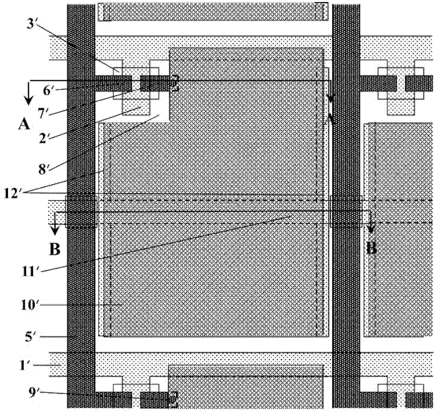
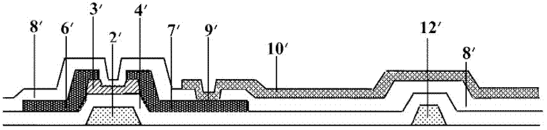
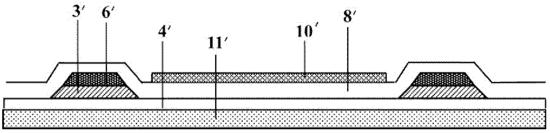
[0038] Such as Figure 4-6 As shown, the TFT-LCD pixel structure of the embodiment of the present invention includes: a substrate on which a common electrode 2, a gate scanning line 3, a gate electrode, a gate insulating layer 4, an active layer 5, a pixel electrode 7, and a source electrode are respectively formed. 8. Patterns of the drain electrode 9 , the data scanning line 13 and the passivation layer 6 , including a second transparent electrode layer 12 . The source electrode 8 and the drain electrode 9 are respectively connected to both ends of the active layer 5, and the drain electrode 9 is connected to the pixel electrode 7. The common electrode 2 is covered with...


PUM

PropertyMeasurementUnit
thicknessaaaaaaaaaa
thicknessaaaaaaaaaa

Abstract

The invention relates to the technical field of liquid crystal display, in particular to a display device, a TFT-LCD (Thin Film Transistor-Liquid Crystal Display) pixel structure and a manufacturing method of the TFT-LCD pixel structure. The TFT-LCD pixel structure comprises a base plate, as well as a common electrode, a grid electrode scanning line, a grid electrode, a grid electrode insulating layer, an active layer, a pixel electrode, a source electrode, a drain electrode, a data scanning line, a passivation layer pattern and a second transparent electrode layer formed on the base plate, wherein the second transparent electrode layer covers at the edge of the pixel electrode, passes through through holes oppositely arranged above the grid electrode scanning line to be connected with the grid electrode scanning line, and forms a storage capacitor with the pixel electrode. According to the display device, the TFT-LCD pixel structure and the manufacturing method of the TFT-LCD pixel structure, the charge of the grid electrode scanning line is stored on the second transparent electrode layer and forms a double-storage capacitance structure together with the common electrode and the first transparent electrode layer on the base plate, so that the storage capacitance is increased greatly, and the display quality of an image is improved effectively.

Description

technical field [0001] The invention relates to the technical field of liquid crystal display, in particular to a display device, a TFT-LCD pixel structure and a manufacturing method thereof. Background technique [0002] In flat panel display technology, TFT-LCD (Thin Film Transistor-Liquid Crystal Display, Thin Film Transistor-Liquid Crystal Display) has the characteristics of low power consumption, relatively low manufacturing cost, and no radiation, so it occupies a dominant position in the flat panel display market . TFT-LCD devices are formed by combining an array substrate and a color filter substrate. Such as Figure 1-3 Shown is a top view of a single pixel of a TFT structure and schematic cross-sectional views of A-A and B-B parts. As shown in the figure, the array substrate includes: a group of gate scanning lines 1' and a group of data scanning lines 5' perpendicular thereto, and adjacent gate scanning lines 1' and data scanning lines 5' define a pixel area . ...

Claims


Application Information

Patent Timeline
Patent Type & Authority Applications(China)
IPC IPC(8): G02F1/1362G02F1/1368H01L27/02H01L21/77
Inventor 张弥
Owner BOE TECH GRP CO LTD
Features
  • R&D
  • Intellectual Property
  • Life Sciences
  • Materials
  • Tech Scout
  • Unparalleled Data Quality
  • Higher Quality Content
  • 60% Fewer Hallucinations
Learn More