Semiconductor device and manufacturing method of semiconductor device
A manufacturing method and semiconductor technology, which are applied in semiconductor/solid-state device manufacturing, semiconductor devices, radiation control devices, etc., can solve problems such as affecting spectroscopic characteristics, affecting wafer yield, and strict allowable position offset in lithography process. Suppress the effect of position shift
- Summary
- Abstract
- Description
- Claims
- Application Information
AI Technical Summary
Problems solved by technology
Method used
Image

Examples
no. 1 Embodiment
[0024] The method of manufacturing a semiconductor device of this embodiment can be applied to, for example, a method of manufacturing a backside illuminated CMOS image sensor. Use the following Figure 1 to Figure 6 The cross-sectional view of the semiconductor device of the present embodiment is described.
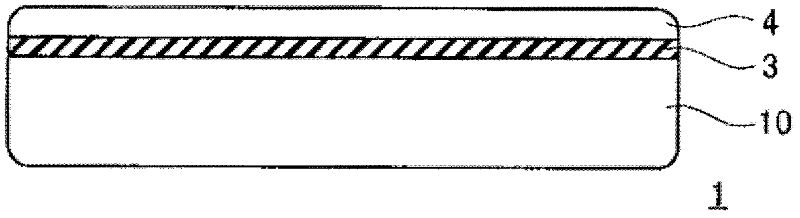
[0025] As the first substrate 1 used as the device wafer, for example, an SOI wafer and / or a single-layer or multi-layer epitaxial (Epitaxial) substrate is used. figure 1 A cross-sectional view showing a case where an SOI wafer is used as the first substrate. The first substrate 1 includes a silicon layer 10 , a BOX oxide film functioning as an etching stop layer 3 to be described later, and a silicon layer 4 .
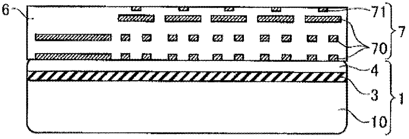
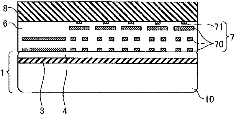
[0026] An active layer (active layer) is formed by repeating a process called FEOL (Front End of Line), such as a photolithography process, a film forming process, an etching process, an ion implantation process, and the like on the silicon layer 4 (photodiode...
no. 2 Embodiment
[0042] The manufacturing method of the semiconductor device of this embodiment can be applied to, for example, the manufacture of a backside illuminated CMOS image sensor. Use the following figure 1 , Figure 7 to Figure 12 The cross-sectional view of the semiconductor device of the present embodiment is described.
[0043] As the first substrate used as a device wafer, such as figure 1 As shown, for example SOI wafers and / or single-layer or multi-layer epitaxial (Epitaxial) substrates are used. The first substrate 1 includes a silicon layer 10 , a BOX oxide film functioning as an etching stop layer 3 to be described later, and a silicon layer 4 .
[0044] An active layer is formed by repeating a process called FEOL (Front End of Line), such as a photolithography process, a film forming process, an etching process, an ion implantation process, etc. on the silicon layer 4 (photodiode layer). Devices such as transistors and / or photodiodes are fabricated in the active layer. ...
PUM
 Abstract
Description
Claims
Application Information
 - R&D Engineer
- R&D Manager
- IP Professional
- Industry Leading Data Capabilities
- Powerful AI technology
- Patent DNA Extraction
Browse by: Latest US Patents, China's latest patents, Technical Efficacy Thesaurus, Application Domain, Technology Topic.
© 2024 PatSnap. All rights reserved.Legal|Privacy policy|Modern Slavery Act Transparency Statement|Sitemap