High voltage isolation structure based on silicon on insulator

A technology of silicon-on-insulator and isolation structure, applied in semiconductor/solid-state device manufacturing, electrical components, circuits, etc., can solve the problem that the sidewall oxide layer cannot be made very thick, shorten the thermal oxidation time, overcome the uneven voltage, Flexible Adjustable Effects

Inactive Publication Date: 2012-09-19
SOUTHEAST UNIV
View PDF5 Cites 7 Cited by
  • Summary
  • Abstract
  • Description
  • Claims
  • Application Information

AI Technical Summary

Problems solved by technology

However, due to process limitations and heat dissipation considerations, the sidewall oxide layer cannot be made very thick

Method used


Image

  • High voltage isolation structure based on silicon on insulator
  • High voltage isolation structure based on silicon on insulator
  • High voltage isolation structure based on silicon on insulator

Examples


Embodiment 1

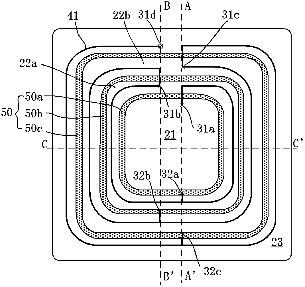
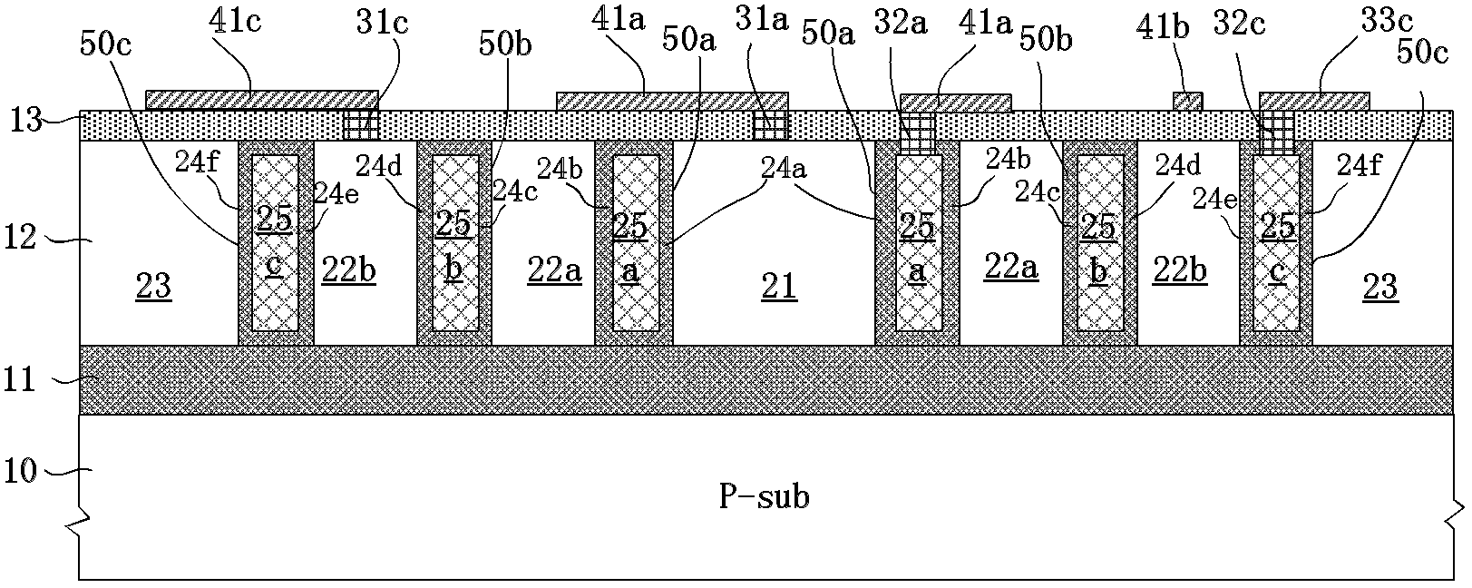
[0023] Embodiment 1 A high-voltage isolation structure based on silicon-on-insulator includes: a P-type substrate 10, a buried oxide layer 11 is provided on the P-type substrate 10, and an N-type epitaxial layer 12 is located above the buried oxide layer 11. The N-type epitaxial layer 12 is provided with a surface passivation layer 13, and the N-type epitaxial layer 12 is provided with a high-voltage circuit area 21 and a low-voltage circuit area 23. The high-voltage circuit area 21 is surrounded by a multi-deep trench isolation structure 50, and the low-voltage circuit area 23 Located outside the multi-deep trench isolation structure 50, the multi-deep trench isolation structure 50 is composed of 2-20 deep trench isolation structures, and a high-resistance polysilicon field plate is provided on the surface passivation layer 13, which is located in the high-voltage circuit area 21 and low-voltage The N-type epitaxial layer of the circuit area 23 is electrically connected to the ...

Embodiment 2

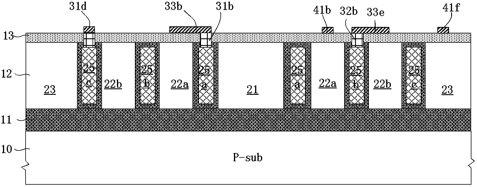
[0031] Embodiment 2 A high-voltage isolation structure based on silicon-on-insulator includes: a P-type substrate 10, a buried oxide layer 11 is provided on the P-type substrate 10, and an N-type epitaxial layer 12 above the buried oxide layer 11, A surface passivation layer 13 is provided on the N-type epitaxial layer 12, a high-resistance polysilicon field plate 41 is provided on the surface passivation layer 13, and a high-voltage circuit area 21 and a low-voltage circuit area 23 are provided in the N-type epitaxial layer 12. The area 21 is surrounded by a three-deep trench isolation structure 50, and the low-voltage circuit area 23 is located outside the three-deep trench isolation structure 50. The three-deep trench isolation structure 50 is composed of a first deep trench isolation structure 50a, a second deep trench isolation structure 50b, and The third deep trench isolation structure 50c is composed of the first deep trench isolation structure 50a adjacent to the high v...

Embodiment 3

[0039] Embodiment 3 Another high-voltage isolation structure based on silicon-on-insulator proposed by the present invention includes: a P-type substrate 10, on which a buried oxide layer 11 is provided, and a N layer above the buried oxide layer 11 Type epitaxial layer 12, a surface passivation layer 13 is provided on the N type epitaxial layer 12, a high resistance polysilicon field plate 42 is provided on the surface passivation layer 13, and a high voltage circuit area 21 and a low voltage The circuit area 23, the high voltage circuit area 21 is surrounded by the double deep groove isolation structure 51, the low voltage circuit area 23 is located outside the double deep groove isolation structure 51, the double deep groove isolation structure 51 is composed of the first deep groove isolation structure 51a, the second The deep trench isolation structure 51b is composed of the first deep trench isolation structure 51a adjacent to the high voltage circuit area 21, the second d...


PUM


Abstract

A high voltage isolation structure based on silicon on an insulator includes that a surface passivation layer is arranged on an N-type epitaxial layer in a silicon structure on the insulator, a high voltage circuit area, a multi-deep-groove isolation structure and a low voltage circuit area are arranged in the N-type epitaxial layer, the high voltage circuit area is enclosed by the multi-deep-groove isolation structure, and the multi-deep-groove isolation structure is composed of 2 to 20 deep groove isolation structures. The high voltage isolation structure is characterized in that a high-resistance polycrystalline silicon field plate is arranged on the surface passivation layer, the N-type epitaxial layer of the high voltage circuit area and the low voltage circuit area is electrically connected with electrode contact holes, and the N-type epitaxial layer between every adjacent deep groove isolation structures is electrically connected with middle electrode contact holes. Two ends of the high-resistance polycrystalline silicon field plate are respectively electrically connected with the electrode contact holes in the high voltage circuit area and the low voltage circuit area, and the high-resistance polycrystalline silicon field plate is sequentially electrically connected with each electrode contact hole from inside to outside.

Description

Technical field [0001] The invention relates to an isolation structure in a high-voltage integrated circuit, which is used to solve the problem of electrical isolation between high and low voltage areas. Background technique [0002] High-voltage power integrated circuits usually refer to circuits that integrate power devices, logic control circuits, and protection circuits on a single silicon chip. Insulator Gate Bipolar Transistor (IGBT) is widely used as a power transistor for power integrated circuits due to its advantages of high current capability and low conduction voltage drop. However, bulk silicon technology is not suitable for integrated IGBTs, because IGBTs have conductivity modulation effects, that is, a large number of minority carriers are injected into the drift region when they are turned on, which will inject carriers into the substrate, which will affect the normality of other circuits in the chip. jobs. The buried oxide layer in the Silicon On Insulator (SOI...

Claims


Application Information

Patent Timeline
Patent Type & Authority Applications(China)
IPC IPC(8): H01L21/762
Inventor 孙伟锋祝靖林颜章钱钦松陆生礼时龙兴
Owner SOUTHEAST UNIV
Why Eureka
Try Eureka