
Component

A component and component technology, applied in the field of packaging of MEMS components, can solve the problems of high risk of contamination or damage

Active Publication Date: 2012-09-19
ROBERT BOSCH GMBH
View PDF6 Cites 28 Cited by
  • Summary
  • Abstract
  • Description
  • Claims
  • Application Information

AI Technical Summary

Problems solved by technology

Furthermore, the larger the through hole in the interposer, the greater the risk that the sensitive diaphragm structure of the MEMS microphone component will be contaminated or damaged during and after the second stage of installation

Method used


Image

  • Component
  • Component
  • Component

Examples


Embodiment Construction

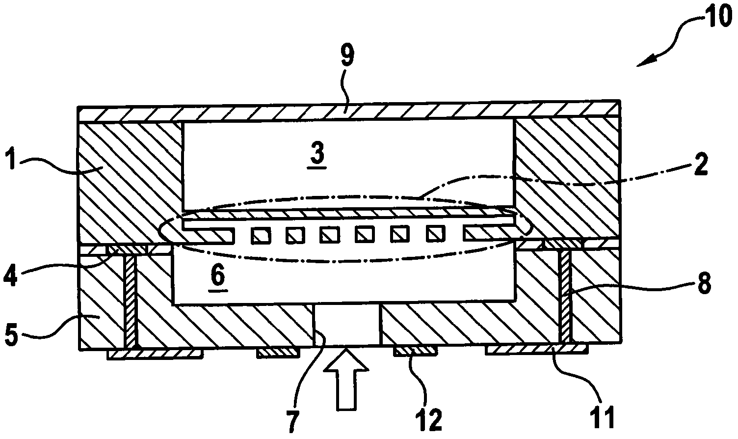
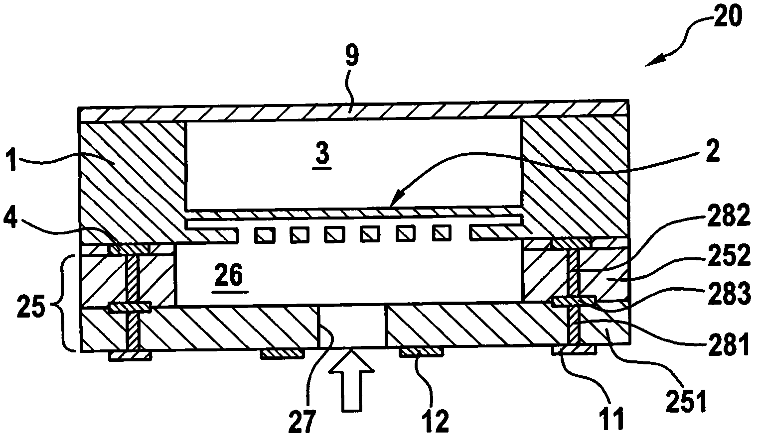
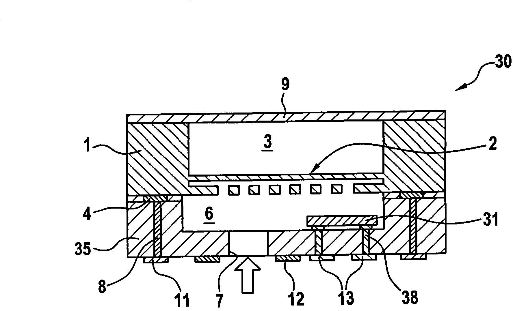
[0019] exist figure 1 The MEMS microphone package 10 shown in is implemented in the form of a wafer level package (WLP), ie in the form of a stack of wafers. The MEMS microphone package 10 includes a microphone component 1 , which is hereinafter referred to as a microphone chip 1 . A sound-sensitive membrane structure 2 in the form of a membrane with a counter-electrode is formed in the front side of the microphone chip 1 and covers the cavity 3 on the rear side of the chip. Usually there are also circuit elements on the front side of the microphone chip, but are not shown here for reasons of clarity. Only the electrical contacts 4 for signal transmission are shown.

[0020] Furthermore, the package 10 includes an interposer 5 which is arranged on the front side of the microphone chip 1 . A groove 6 is formed in the surface of the interposer 5 facing the microphone chip 1 , which groove extends over the entire diaphragm area. The interposer 5 can be, for example, a backsi...


PUM


Abstract

A wafer-level-based packaging concept for MEMS components having at least one diaphragm structure formed in the component front side is described, according to which an interposer is connected to the front side of the MEMS component, which has at least one passage aperture as an access opening to the diaphragm structure of the MEMS component and which is provided with electrical through contacts so that the MEMS component is electrically contactable via the interposer. The cross-sectional area of the at least one passage aperture in the interposer is to be designed as significantly smaller than the lateral extension of the diaphragm structure of the MEMS component. The at least one passage aperture opens into a cavity(6) between the diaphragm structure (2) and the interposer(5).

Description

technical field [0001] The invention generally relates to the packaging of MEMS (Micro Electro Mechanical Systems) components within the scope of wafer-level AVT (Assembly and Connectivity Technology), and in particular to the packaging of MEMS components with a membrane structure formed in the front side of the component. Such components can be, for example, pressure sensor, loudspeaker or microphone components. These applications require media channels in the package. Background technique [0002] On the one hand, the packaging of the MEMS components serves for the mechanical protection of the chip. On the other hand, said encapsulation enables the mechanical and electrical connection of components within the context of a second level of mounting, for example on a printed circuit board. In practice, printed circuit board-based packages or ceramic housings are mostly used as packages for MEMS components. These two packaging schemes are accompanied by relatively high manu...

Claims


Application Information

Patent Timeline
Patent Type & Authority Applications(China)
IPC IPC(8): H04R19/04B81B3/00
CPCH04R19/04B81B7/0061B81B7/02B81B2207/095B81B3/00H04R19/005H04R31/00
Inventor J·策尔兰R·艾伦普福特U·肖尔茨
Owner ROBERT BOSCH GMBH
Learn More