Flexible transparent conductive film and manufacturing method thereof

A technology of transparent conductive film and manufacturing method, which is applied in the direction of cable/conductor manufacturing, conductive layer on insulating carrier, circuit, etc., and can solve the problem of high resistance of flexible transparent conductive film, thick printing thickness of transparent ink, and poor dispersion of nano-silver wires Good and other problems, to achieve the effect of improving mechanical stability, good electrical conductivity, and high binding force

Active Publication Date: 2016-01-20
SHENZHEN GRADUATE SCHOOL TSINGHUA UNIV
View PDF12 Cites 0 Cited by
  • Summary
  • Abstract
  • Description
  • Claims
  • Application Information

AI Technical Summary

Problems solved by technology

[0004] There are two structures in the existing flexible transparent conductive film, one is a three-layer separation structure: a flexible transparent substrate, a transparent ink layer, and a nano-silver wire layer in sequence. In this three-layer structure, the transparent ink layer is coated on the flexible transparent substrate. , the nano-silver wire layer is set on the surface of the transparent ink layer, there is no chemical bond between the nano-silver wire layer and the transparent ink layer, it is only combined by van der Waals force between molecules, this bonding force is relatively weak, flexible and transparent when touched It is easy to knock off the silver nano wire layer on the surface of the conductive film
[0005] Another structure is that the flexible transparent conductive film has a two-layer structure, followed by a flexible transparent substrate and a transparent ink conductive layer. The transparent ink conductive layer is made by mixing nano-silver wires with transparent ink and printing on the surface of the flexible transparent substrate. The dispersion of nano-silver wires in transparent ink is not good, and the printing thickness of transparent ink is relatively thick, nano-silver wires cannot form a two-dimensional conductive network in transparent ink, so the resistance of flexible transparent conductive film is correspondingly high, and the guiding performance is not good. it is good
[0006] In addition, the nano-silver wires prepared by the prior art have a very high aspect ratio (greater than 100), so there are certain technical difficulties when coating to form a uniform film, and the nano-silver wires are only separated by weaker molecules. The force between them is overlapped together, and it is easy to slip under the action of flexure, so the contact resistance is higher and less stable

Method used


Image

  • Flexible transparent conductive film and manufacturing method thereof
  • Flexible transparent conductive film and manufacturing method thereof
  • Flexible transparent conductive film and manufacturing method thereof

Examples


Embodiment 1

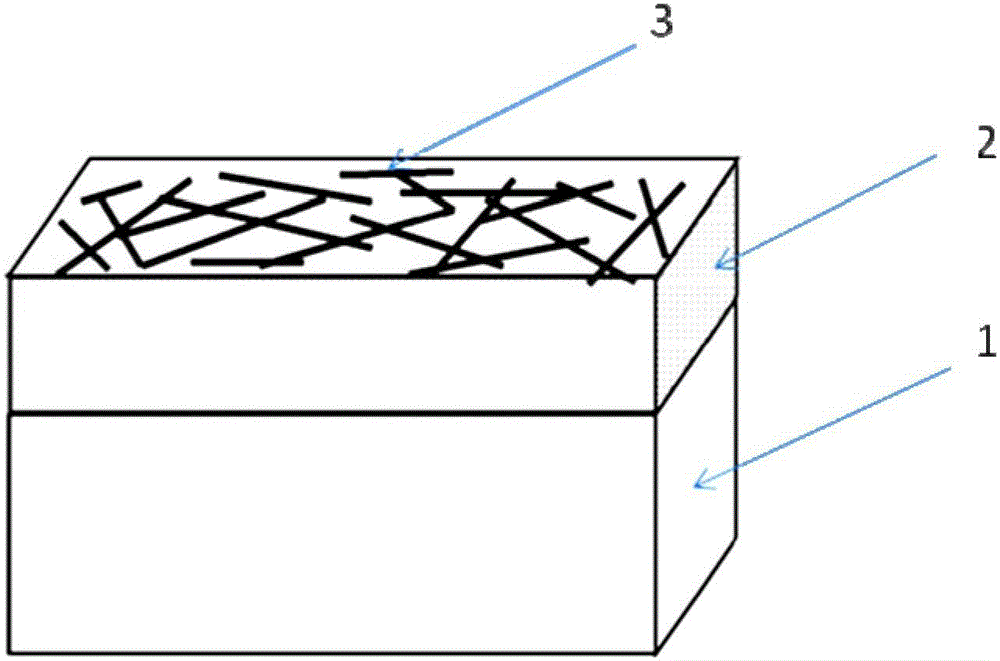
[0029] Example 1, such as figure 1 As shown, a flexible transparent conductive film is a sheet-like multilayer structure, including a flexible transparent substrate 1, which is the supporting base layer of the entire conductive film. The surface of the flexible transparent substrate 1 is coated with a transparent ink layer 2 formed by transparent ink, the surface layer of the transparent ink layer 2 is a conductive layer 3 adhered with silver nanowires, and the silver nanowires in the conductive layer 3 overlap each other connected to form a uniform two-dimensional silver nanowire network. Since nano-silver wires are distributed on the surface layer of transparent ink layer 2 by hot pressing or transfer printing, the network of nano-silver wires in conductive layer 3 can be a good seepage network thin layer, and nano-silver wires are adhesive Attached to the surface layer of the transparent ink layer 2; therefore, its two-dimensional conductive properties will not be affected...

Embodiment 2

[0040] Embodiment 2, a kind of manufacturing method of flexible transparent conductive film, comprises the following steps:

[0041] (1) Choose a flexible transparent substrate. The requirement for a flexible transparent substrate is to be thermoplastic and transparent in the visible light region. Therefore, materials that meet this condition can be used to manufacture flexible transparent substrates. Specifically preferred is a flexible transparent substrate made of polyethylene phthalate, polybutylene phthalate, polyethylene naphthalate or polycarbonate, and the size and shape of the flexible transparent substrate will be manufactured according to actual conditions. The size of the conductive film is determined. Print or coat the transparent ink evenly on the flexible transparent substrate, dry or cure the transparent ink, the drying can be natural drying or heating drying, the drying temperature is from room temperature to 180°C, so that the transparent ink can firmly adher...

Embodiment 2-10 to Embodiment 2-15

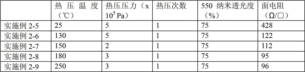
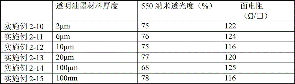
[0058] Examples 2-10 to 2-15 were manufactured using the steps of Example 2 above, and the specific materials and experimental conditions were as follows: the material of the flexible transparent substrate was polycarbonate (purchased from DuPont Teijin Melinix, with a thickness of 80 μm), The material of the transparent ink is polyethylene glycol butyral (the number average molecular weight is 1 million, the glass transition temperature is 72 ℃), the average diameter of the nano-silver wire is 80 nanometers, and the average length is 8 μm. The concentration is 0.42wt%, and the flexible substrate coated with silver nanowires is polyethylene phthalate (thickness 12 μm). The drying condition is to dry at 80°C for 15 minutes. The hot pressing temperature is 130°C, and the hot pressing pressure is 5x10 5 Pa, the number of times of hot pressing is one time. The obtained results are listed in Table 3.

[0059] Table 3 The relationship between the thickness of transparent ink and ...


PUM

PropertyMeasurementUnit
thicknessaaaaaaaaaa
diameteraaaaaaaaaa
thicknessaaaaaaaaaa

Abstract

The invention discloses a flexible transparent electric conducting film and a manufacturing method thereof. The electric conducting film comprises a flexible transparent base plate, wherein a transparent oil ink layer is coated on the surface of the flexible transparent base plate; the surface layer of the transparent oil ink layer is an electric conducting layer pasted with nano silver wires; and the nano silver wires in the electric conducting layer are mutually overlapped so as to form a uniform two-dimensional nano silver wire network. The preparation method comprises the following steps of: printing or coating the transparent oil ink on the flexible transparent base plate; coating a nano silver wire dispersing liquid uniformly on the surface of another flexible transparent base plate so as to obtain a nano silver wire thin film; and through a hot pressing or transfer printing mode, transferring and pasting the thin film to the surface layer of the transparent oil ink so as to obtain the flexible transparent electric conducting film. The electric conducting film surface provided by the invention is lower in resistance value and is high in bonding force of each layer, has favorable contact, and has good uniformity; and the preparation method is simple in technology and is low in cost, and can prepare large-area transparent electric conducting films, and the prepared transparent electric conducting film has favorable electric conducting performance.

Description

technical field [0001] The invention belongs to the field of microelectronic material preparation technology. It relates to a conductive film and a manufacturing method thereof, in particular to a flexible transparent conductive film and a manufacturing method thereof. Background technique [0002] Transparent conductive films have been widely used in various display screens and solar cells and other fields. At present, the most widely used is a conductive transparent electrode made of a transparent conductive film, and the main material of the transparent conductive film is indium tin oxide (ITO). Since the ITO film must be prepared by a vacuum magnetic sputtering process, this process and equipment restrict the area of ​​the manufactured transparent conductive film, which is not conducive to large-area continuous manufacturing. In addition, as a metal oxide, indium tin oxide is not resistant to bending and bending, so it cannot be used in flexible electronic devices. ...

Claims


Application Information

Patent Timeline
Patent Type & Authority Patents(China)
IPC IPC(8): H01B5/14H01B13/00
Inventor 杨诚吴浩怡李宝华康飞宇
Owner SHENZHEN GRADUATE SCHOOL TSINGHUA UNIV
Why Eureka
Try Eureka