Positron emission tomography detector for multilayer scintillation crystal
A technology of positron emission and scintillation crystals, which is applied in the field of detector devices, can solve the problems that detectors cannot be mass-produced and reference data is time-consuming and labor-intensive, and achieve the effects of improving spatial resolution, improving imaging quality, and high detection efficiency
- Summary
- Abstract
- Description
- Claims
- Application Information
AI Technical Summary
Problems solved by technology
Method used
Image
Examples
Embodiment 1
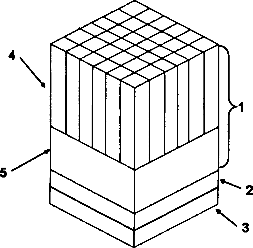
[0044] Such as figure 1 As shown, the multilayer scintillation crystal PET detector includes a multilayer scintillation crystal 1 , a photodetector system 2 and an algorithm system 3 . Among them, the multi-layer scintillation crystal 1 is composed of two layers of scintillation crystals, the top layer of scintillation crystal 4 is an array scintillation crystal, and the bottom layer of scintillation crystal 5 is a continuous scintillation crystal; the connected surfaces of the two layers of scintillation crystals are coupled together by optical glue. The scintillation crystal 4 on the top layer is in the shape of a cube, which is composed of 6×6 scintillation crystal strips of the same size spliced on the horizontal plane. The bottom surface of the underlying scintillation crystal 5 is directly coupled with the photodetector system 2 . The photodetector system 2 is composed of 4×4 SiPMs. The scintillation crystal 5 on the bottom layer has a height of 1 mm, and the scintil...
Embodiment 2
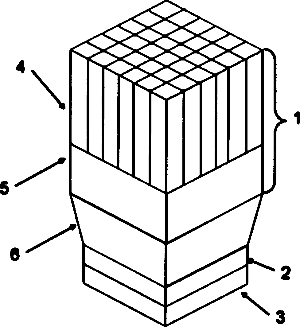
[0046] Such as figure 2 As shown, the multilayer scintillation crystal PET detector includes a multilayer scintillation crystal 1, a photodetector system 2 and an algorithm system 3, wherein the multilayer scintillation crystal 1 is composed of two layers of scintillation crystals, and the top layer of scintillation crystals 4 is an array scintillation crystal, The scintillation crystals 5 at the bottom layer are continuous scintillation crystals; the connected surfaces of the two layers of scintillation crystals are coupled together by optical glue and have exactly the same shape and size. The scintillation crystal 4 on the top layer is in the shape of a cube, which is composed of 6×6 scintillation crystal strips of the same size spliced on the horizontal plane. The bottom surface of the underlying scintillation crystal 5 is coupled with the photodetector system 2 through the light guide 6 . The photodetector system 2 is composed of 4×4 SiPMs. The scintillation crystal 5...
Embodiment 3
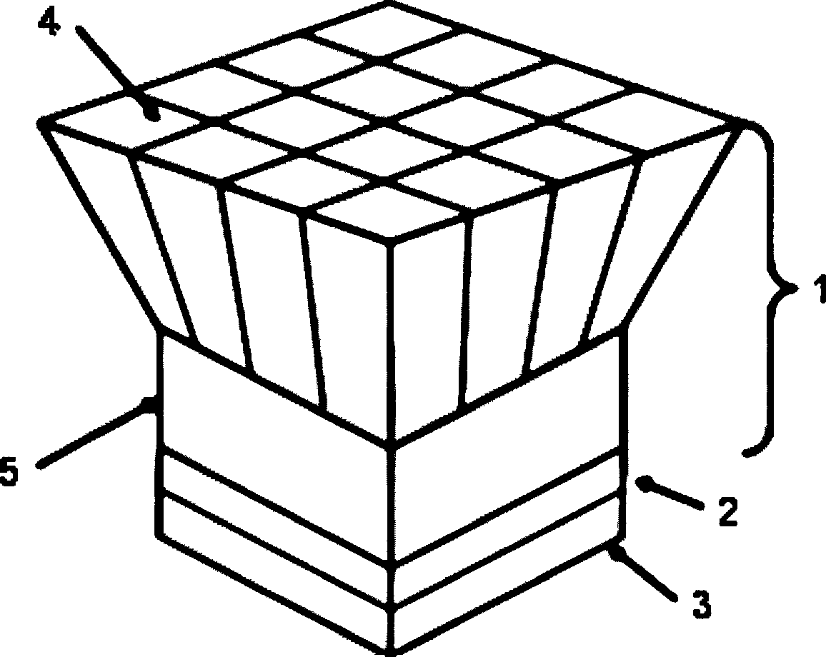
[0048] Such as image 3As shown, the multilayer scintillation crystal PET detector includes a multilayer scintillation crystal 1, a photodetector system 2 and an algorithm system 3, wherein the multilayer scintillation crystal 1 is composed of two layers of scintillation crystals, and the top layer of scintillation crystals 4 is an array scintillation crystal, The scintillation crystals 5 at the bottom layer are continuous scintillation crystals; the connected surfaces of the two layers of scintillation crystals are coupled together by optical glue. The appearance shape of the scintillation crystals 4 on the top layer is a truncated cone. The top surface and the bottom surface of the array scintillation crystals are parallel to each other, and are composed of 4×4 scintillation crystal strips spliced on the horizontal plane. The bottom surface of the underlying scintillation crystal 5 is coupled with the photodetector system 2 through optical glue. The scintillation crystal ...
PUM
 Abstract
Description
Claims
Application Information


