Penta band antenna of PCB (printed circuit board)

A PCB board and antenna technology, applied in the field of PCB five-frequency antenna, can solve the problems of single technology, unfavorable miniaturization, and antenna cost cannot be further reduced, and achieve low antenna cost, improved radiation problem, and thin and small effect

Inactive Publication Date: 2012-10-03
GUANGDONG BUBUGAO ELECTRONICS IND
View PDF4 Cites 3 Cited by
  • Summary
  • Abstract
  • Description
  • Claims
  • Application Information

AI Technical Summary

Problems solved by technology

[0002] The technology of common PIFA antennas to achieve multi-band coverage is relatively simple. For example, five-band antennas generally require an antenna height of 6-8mm and an antenna area of ​​600-800mm2. The structure is usually realized by steel sheet, FPC, LDS and other process materials.
The height requirement of the antenna restricts the thickness of the mobile terminal, which is not conducive to the miniaturization requirement, and the cost of the antenna cannot be further reduced
At present, there are not many researches on PCB multi-frequency antennas. Under the same clearance area, the bandwidth of PCB antennas is much narrower than that of ordinary antennas. As a result, PCB antennas require a large clearance area to achieve the performance of ordinary antennas, which is not conducive to the layout of mobile terminal motherboards. Traces

Method used


Image

  • Penta band antenna of PCB (printed circuit board)
  • Penta band antenna of PCB (printed circuit board)
  • Penta band antenna of PCB (printed circuit board)

Examples


Embodiment Construction

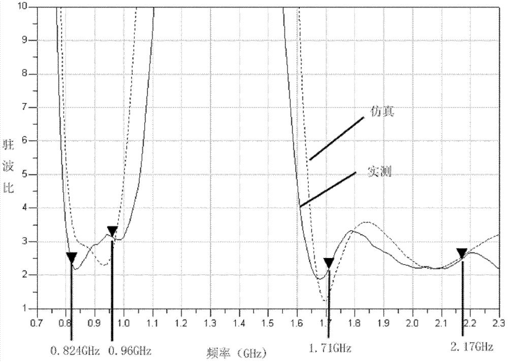
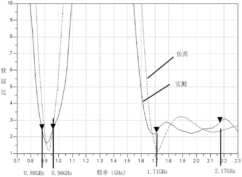
[0019] The present invention will be described in detail below in conjunction with accompanying drawing, but not as limiting the present invention:

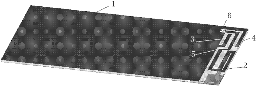
[0020] Such as figure 1 As shown, this embodiment includes a ground plane 1, a feed point 6, a main radiator 2, at least one matching element 5, a first ground parasitic sheet 3 and a second ground parasitic sheet 4, and the main radiator 2 is designed One end of the strip line on the PCB is electrically connected to the feed point 6, and the first ground parasitic sheet 3 and the second ground parasitic sheet 4 are respectively arranged on both sides of the main radiator 2, And electrically connected to the ground plane 1 , at least one matching element 5 is connected in parallel to the ground plane 1 in the middle of the main radiator 2 , and the remaining matching elements 5 form pi-shaped matching at the feed point 6 .

[0021] There are two parasitic units, located on both sides of the main radiator, which determine the sec...


PUM


Abstract

The invention discloses a penta band antenna of a PCB (printed circuit board). The penta band antenna comprises a grounding plane, a feeding point, a main radiating body, at least one matching element, a first grounded parasitic tablet and a second grounded parasitic tablet, wherein the main radiating body is a strip line arranged on the PCB; one end of main radiating body is electrically connected to the feeding point; the first grounded parasitic tablet and a second grounded parasitic tablet are respectively arranged at the two edges of the main radiating body and electrically connected to the grounding plane; at least one matching element is connected to the grounding plane in parallel at the middle section of the main radiating body, and the other matching elements form into the pi-shaped match at the feeding point. The penta band antenna can be widely applied to an ultra-thin mobile terminal of an antenna with a proper clearance area.

Description

(1) Technical field: [0001] The invention belongs to the field of antennas for electronic mobile terminals, and in particular relates to a PCB five-frequency antenna. (two) background technology: [0002] Ordinary PIFA antennas have relatively simple technology to achieve multi-band coverage. For example, five-band antennas generally require antenna heights of 6-8mm and antenna areas of 600-800mm2. Steel sheets, FPC, LDS and other process materials are often used for structural implementation. The height requirement of the antenna restricts the thickness of the mobile terminal, which is not conducive to the miniaturization requirement, and the cost of the antenna cannot be further reduced. At present, there are not many researches on PCB multi-frequency antennas. Under the same clearance area, the bandwidth of PCB antennas is much narrower than that of ordinary antennas. As a result, PCB antennas require a large clearance area to achieve the performance of ordinary antennas,...

Claims


Application Information

Patent Timeline
IPC IPC(8): H01Q1/38H01Q1/48H01Q5/01H01Q5/10
Inventor 陈玉稳
Owner GUANGDONG BUBUGAO ELECTRONICS IND
Why Eureka
Try Eureka