Silicon-based broadband wide-angle scanning antenna unit

An antenna unit, wide-angle scanning technology, applied in the direction of the connection of the antenna grounding switch structure, the structure of the radiating element, etc., can solve the problem that the radiation efficiency of the all-silicon integrated antenna unit cannot meet the general application requirements, the processing accuracy is high, and the dielectric The problem of high electrical constant can reduce the integration accuracy requirements, reduce the antenna profile, and reduce the cost of the antenna.

Pending Publication Date: 2021-01-29
CHINA ELECTRONICS TECH GRP CORP NO 14 RES INST
View PDF0 Cites 1 Cited by
  • Summary
  • Abstract
  • Description
  • Claims
  • Application Information

AI Technical Summary

Problems solved by technology

The working wavelength corresponding to the 60GHz frequency band and the corresponding circuit size are small, and the requirements for processing accuracy are relatively high, especially in the application of the phased array system, the circuit size of the radiation unit and the like needs to meet the half-wavelength limit. The cost poses a great challenge
However, the traditional silicon-based process has a high dielectric constant and large loss, and the radiation efficiency of the all-silicon-based integrated antenna unit will not meet the general application requirements.

Method used


Image

  • Silicon-based broadband wide-angle scanning antenna unit
  • Silicon-based broadband wide-angle scanning antenna unit
  • Silicon-based broadband wide-angle scanning antenna unit

Examples


Embodiment 1

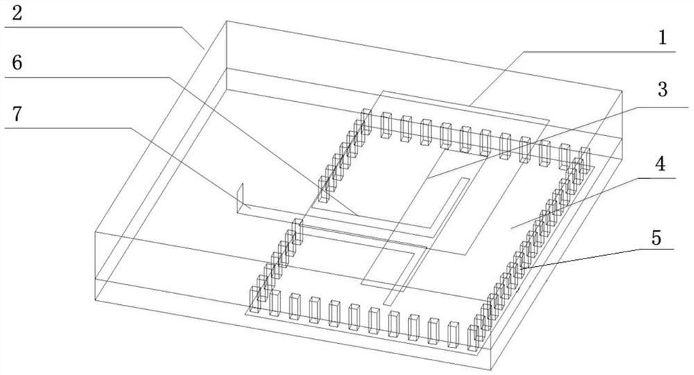
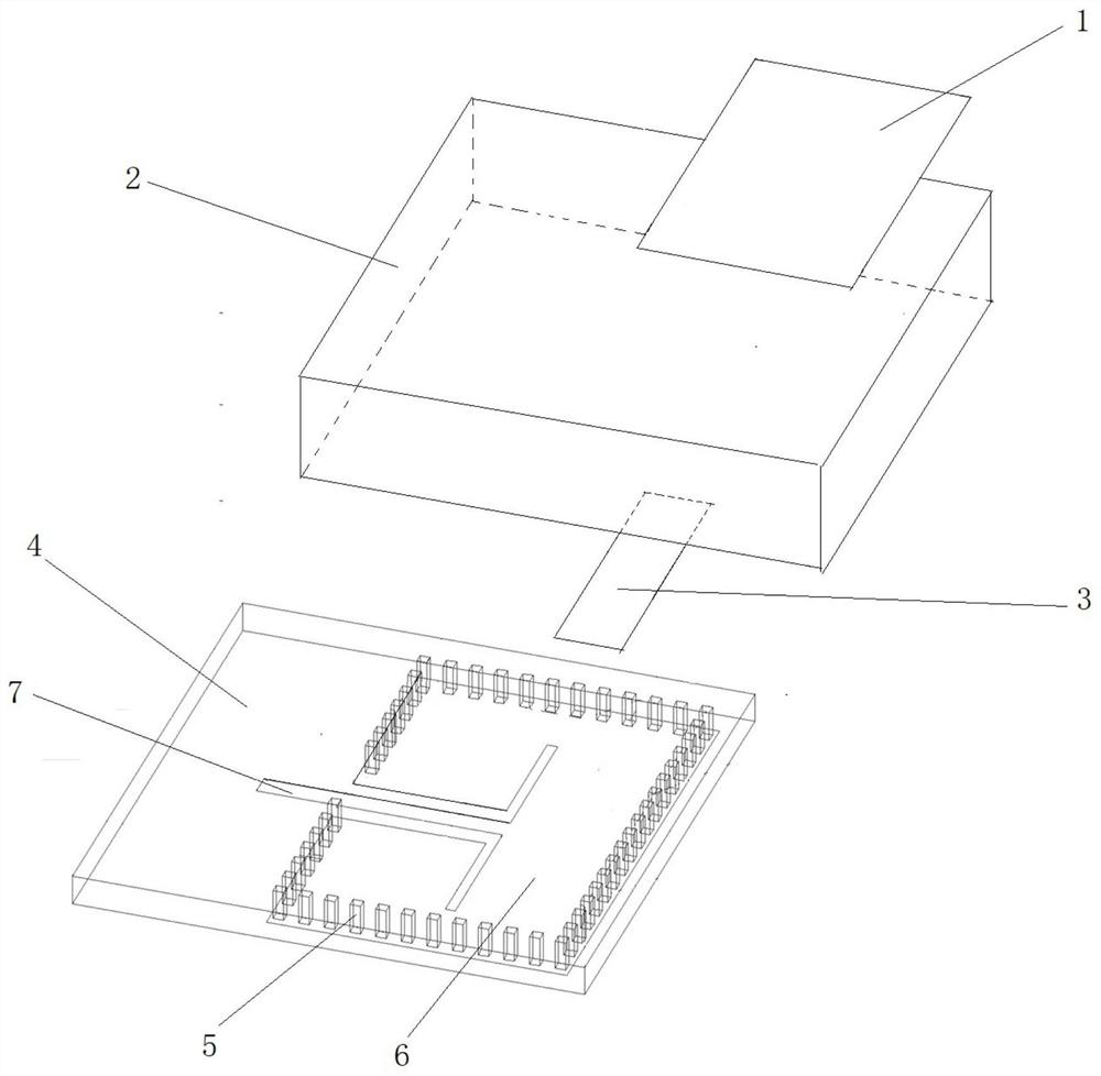
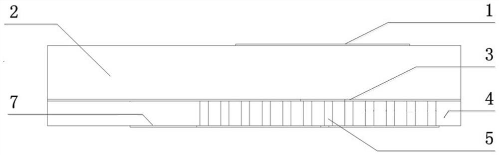
[0027] combine Figure 1-Figure 5 The silicon-based wide-bandwidth angular scanning antenna unit of this embodiment consists of a rectangular patch 1, a glass substrate 2, a slot-coupled feeding layer 3, a silicon-based substrate integrated waveguide back cavity 4, and an impedance transformation layer 6 from top to bottom. The slot coupling feeding layer 3 is provided with a rectangular hollow part, and the rectangular hollow part is covered by the rectangular patch 1 in the vertical direction; The base metallization shielding via hole 5, the silicon base metallization shielding via hole 5 is a hollow or solid cylinder made of metal; the silicon base metallization shielding via hole 5 will connect the gap coupling feed layer 3 and impedance transformation Layer 6 is connected, and the impedance transformation layer 6 is a common-ground coplanar waveguide structure, and the strip-shaped extension part in the middle is a microstrip feeding transmission line 7 . In this embodim...


PUM

PropertyMeasurementUnit
sizeaaaaaaaaaa

Abstract

The invention discloses a silicon-based broadband wide-angle scanning antenna unit which consists of a rectangular patch 1, a glass substrate 2, a slot coupling feed layer 3, a silicon-based substrateintegrated waveguide back cavity 4 and an impedance conversion layer 6 from top to bottom. A silicon-based metallized shielding through hole 5 penetrating through the upper surface and the lower surface of the silicon-based substrate integrated waveguide back cavity 4 is formed in the silicon-based substrate integrated waveguide back cavity 4; and the silicon-based metallized shielding through hole 5 connects the connecting slot coupling feed layer 3 with the impedance conversion layer 6, the impedance conversion layer 6 is a common-ground coplanar waveguide structure, and a middle strip-shaped extension part is a microstrip feed transmission line 7. The silicon-based broadband wide-angle scanning antenna unit disclosed by the invention is realized by adopting a standardized glass substrate, a silicon substrate and a standardized wiring, through hole and copper-tin bonding process so that the process complexity and the processing cost are reduced, and the whole structure has the advantages of a low profile, high reliability, a simple process, low cost and the like.

Description

technical field [0001] The invention belongs to the technical field of microwave antennas, in particular to a silicon-based wide bandwidth angle scanning antenna unit. Background technique [0002] With the depletion of wireless communication frequency band resources below 6GHz, the millimeter wave frequency band has become an inevitable trend in the development of wireless communication. Millimeter wave spectrum resources include frequency bands from 30 GHz to 300 GHz, which can be divided into "atmospheric window" and "non-atmospheric window" according to atmospheric attenuation, corresponding to the minimum and maximum frequency ranges of attenuation respectively. In addition to the "atmospheric window" frequency band, which is more suitable for long-distance wireless transmission, the "non-atmospheric window" frequency band has also received extensive attention and research because of its advantages in confidentiality and frequency reuse. Spectrum resources near 60GHz (...

Claims


Application Information

Patent Timeline
Patent Type & Authority Applications(China)
IPC IPC(8): H01Q1/38H01Q1/50
CPCH01Q1/38H01Q1/50
Inventor 周浩孙磊王侃
Owner CHINA ELECTRONICS TECH GRP CORP NO 14 RES INST
Why Eureka
Try Eureka