Array substrate, display device and method for driving array substrate

An array substrate and driving voltage technology, which is applied in static indicators, nonlinear optics, instruments, etc., can solve the problems of high driving voltage and large power consumption

Active Publication Date: 2012-10-24
BOE TECH GRP CO LTD
View PDF5 Cites 38 Cited by
  • Summary
  • Abstract
  • Description
  • Claims
  • Application Information

AI Technical Summary

Problems solved by technology

[0006] The driving voltage of the existing pixel electrode and common elec

Method used


Image

  • Array substrate, display device and method for driving array substrate
  • Array substrate, display device and method for driving array substrate
  • Array substrate, display device and method for driving array substrate

Examples


Embodiment 1

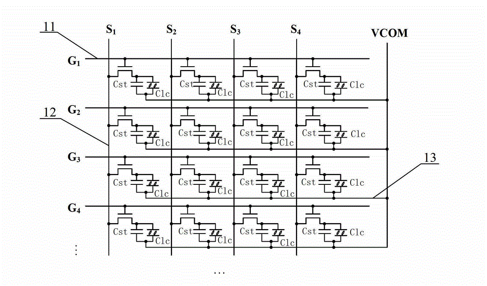
[0070] An embodiment of the present invention provides an array substrate, image 3 Wiring the TFT array of the array substrate, including:

[0071] Several pixel units 14, the pixel units 14 include thin film transistors, pixel electrodes and common electrodes, for displaying images;

[0072] Several gate lines 11 (G 1 ~G n ), wherein each gate line 11 is connected to the gate of a thin film transistor in a row of pixel units 14, and provides a gate scanning signal to the pixel unit 14;

[0073] Several data lines 12 (S 1 ~S n ), wherein each data line 12 is connected to a pixel electrode in a row of pixel units 14 through the thin film transistor, and provides data signals to the pixel unit 14;

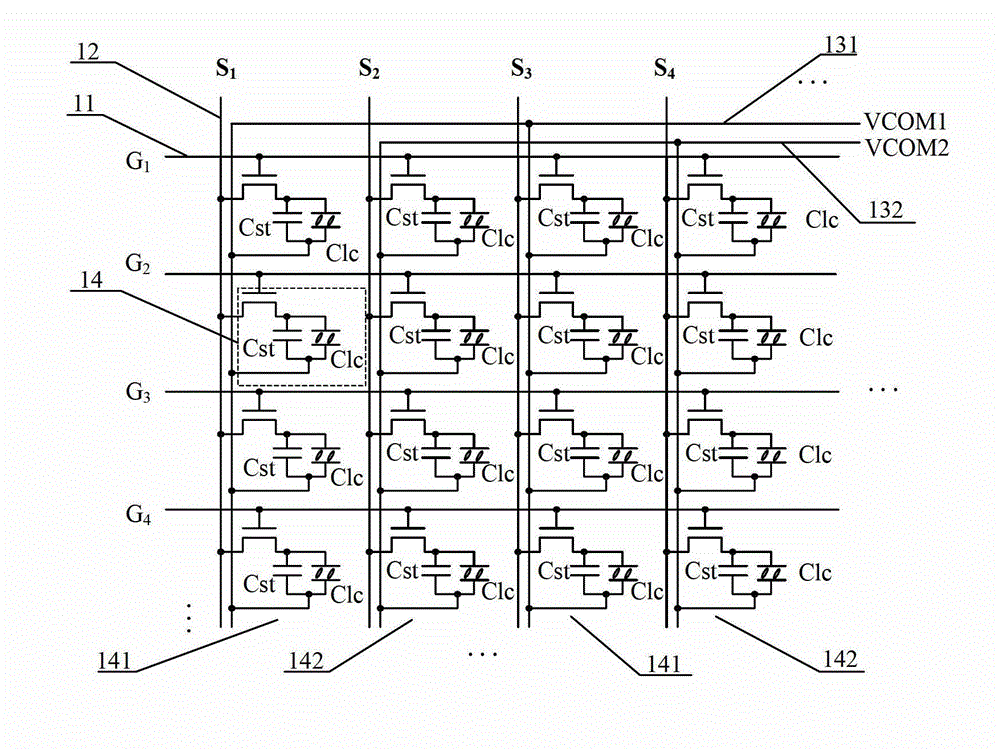
[0074] A plurality of first common electrode lines 131 and a plurality of second common electrode lines 132 are connected to common electrodes in the pixel unit 14, wherein each first common electrode line 131 is connected to an odd column of pixel units 141, and each second co...

Embodiment 2

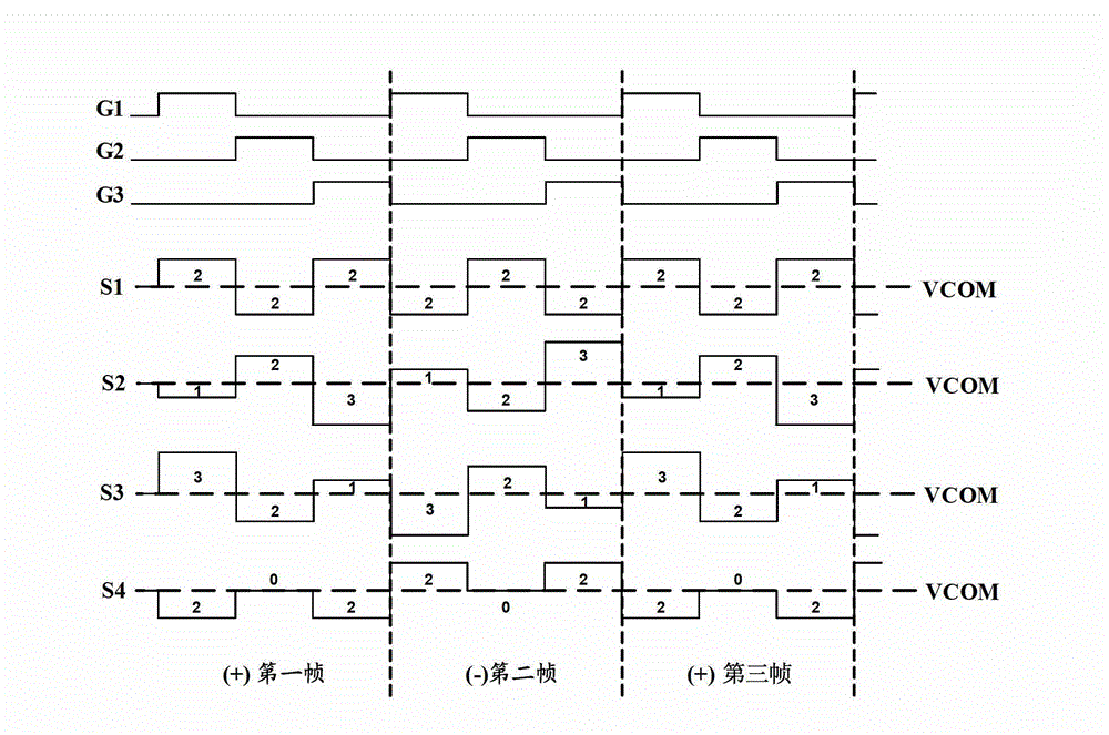
[0104] Based on the array substrate described in Embodiment 1, an embodiment of the present invention provides a method for driving the array substrate, such as Figure 10 As shown, the method includes:

[0105] Step 101, when displaying a frame of pictures, turn on each row of pixel units sequentially through the gate lines;

[0106] Step 102, when the pixel units in each row are turned on, apply the opposite driving voltage difference to the pixel units in the odd columns and the pixel units in the even columns respectively through the data line and the first common electrode line or the second common electrode line, wherein, loading The polarity of the common voltage applied to the pixel units in odd columns is opposite to that applied to the pixel units in even columns, and the polarity of the driving voltage difference applied to any pixel unit is opposite to the polarity of the common voltage applied to the pixel unit.

[0107]In the method for driving the array substra...


PUM


Abstract

The invention discloses an array substrate, a display device and a method for driving the array substrate, relates to the display field, can realize polarity inversion, and also can effectively reduce driving voltage of a pixel electrode and a public electrode so as to realize a purpose of reducing consumption of electric quality. The array substrate comprises a plurality pixel units, a plurality of grid lines, a plurality of data lines, a plurality of first public electrode lines and a plurality of second public electrode lines, wherein the plurality of grid lines are used for providing grid scanning signals for the pixel units; the plurality of data lines are used for providing data signals for the pixel units; each first public electrode line is connected with an odd-column of pixel units, each second public electrode line is connected with an even-column of pixel units, public voltages with inverse polarities are respectively provided for the odd-column of pixel units and the even-column of pixel units, and the polarity of driving voltage difference loaded to any one pixel unit by using the data lines and the first/second public electrode lines is opposite to the polarity of the public voltage loaded to the pixel unit.

Description

technical field [0001] The present invention relates to the field of liquid crystal display, in particular to an array substrate, a display device and a method for driving the array substrate. Background technique [0002] The liquid crystal display device is a device widely used in various electronic devices. Its display principle is to apply a voltage difference to the liquid crystal molecules. The voltage difference generates an electric field to drive the liquid crystal molecules to deflect. The degree of deflection of the liquid crystal molecules is controlled by the magnitude of the applied voltage difference. , so as to control the brightness and darkness of the light emitted through the liquid crystal layer to display images, and the voltage difference (driving voltage difference) applied to the liquid crystal molecules must be reversed at regular intervals to avoid polarization of the liquid crystal material. Cause permanent damage, and also to avoid image residual ...

Claims


Application Information

Patent Timeline
IPC IPC(8): G02F1/1362G02F1/1368G02F1/133G09G3/36
CPCG02F1/1362G09G3/36G02F1/133G02F1/1368G09G3/3688G09G3/3614G09G3/3655G09G2310/027G09G2330/021
Inventor 史世明李云飞石领
Owner BOE TECH GRP CO LTD
Why Eureka
Try Eureka