

Test construction for transistor
A technology for testing structures and transistors, which is applied in the direction of electrical solid-state devices, semiconductor devices, semiconductor/solid-state device components, etc., and can solve problems such as deviation from the standard value range and damage
- Summary
- Abstract
- Description
- Claims
- Application Information
AI Technical Summary
Problems solved by technology
Method used
Image

Examples
no. 1 example
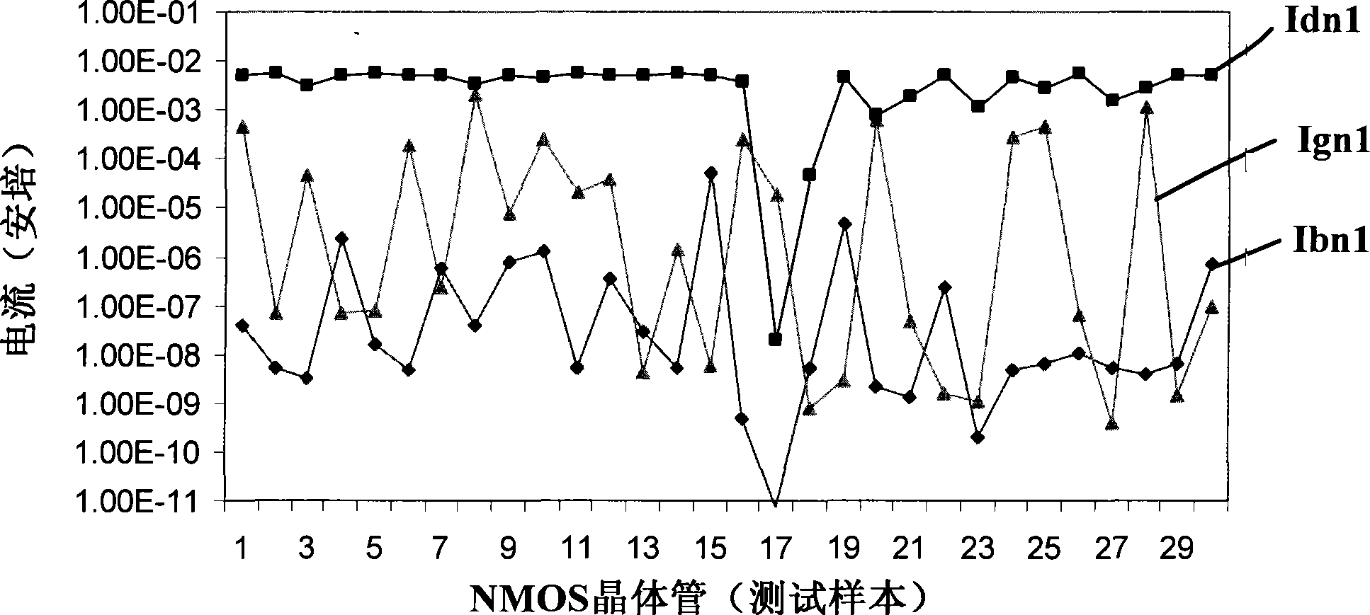
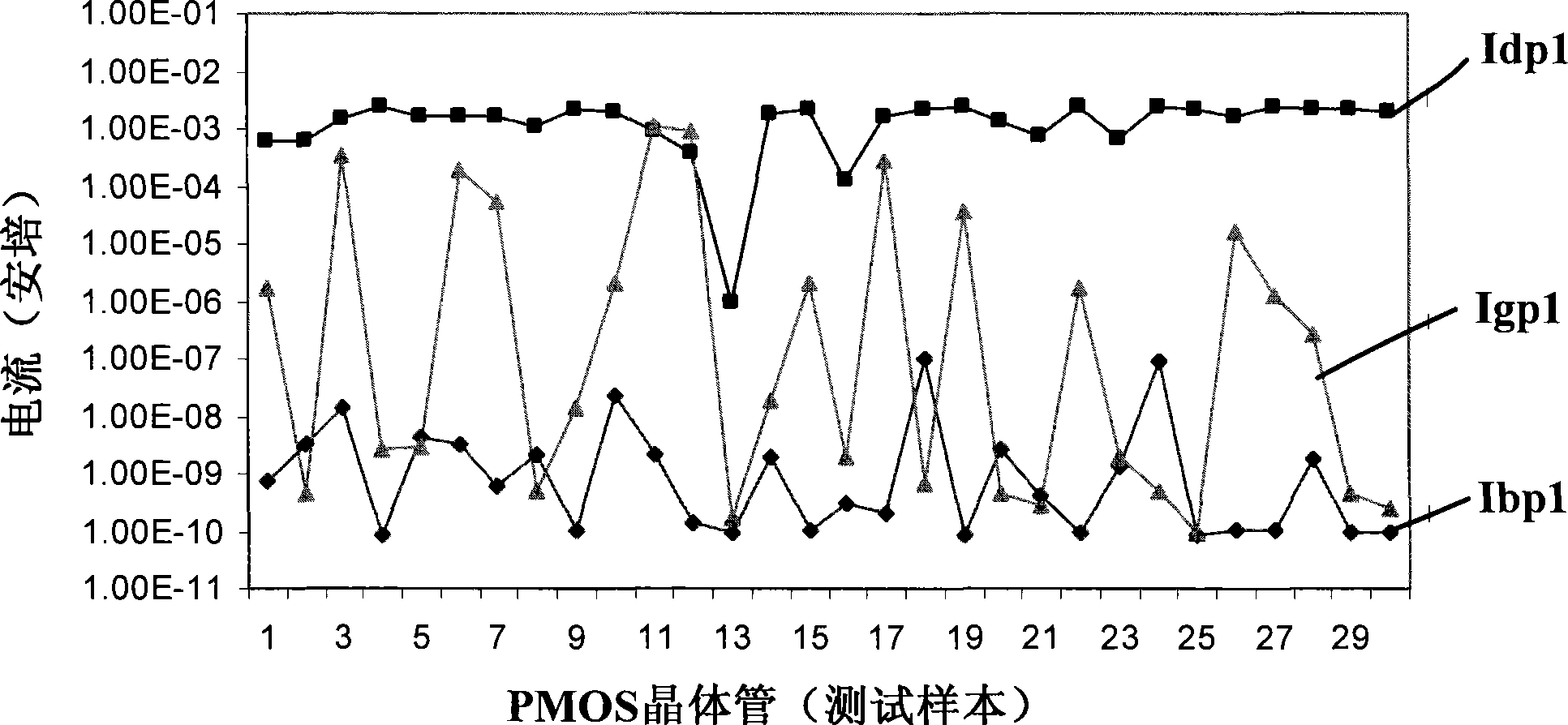
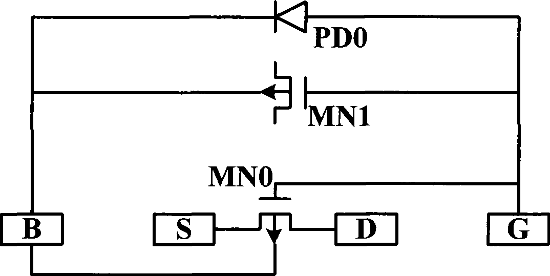
[0028] Please refer to image 3 , the test structure of the transistor in this embodiment includes a test transistor MN0, a protection transistor MN1 and a diode PD0.
[0029] In this embodiment, the test transistor MN0, that is, the transistor to be tested is an NMOS transistor. The protection transistor MN1 is used as a charge storage element to connect the gate G of the test transistor MN0 to the substrate B, that is, the gate of the protection transistor MN1 is connected to the gate G of the test transistor MN0, and the substrate of the protection transistor MN1 is connected to the substrate of the test transistor MN0 B connection, the protection transistor MN1 has the function of communicating AC and blocking DC, and the protection transistor MN1 is an NMOS transistor. The diode PD0 is used as a discharge element to connect the gate G of the test transistor MN0 and the substrate B, and the diode PD0 has the function of communicating AC and blocking DC. Therefore, the pr...
no. 2 example
[0039] Please continue to refer Figure 5 The difference between this embodiment and the first embodiment is that in this embodiment, a parallel plate capacitor C1 is used as a charge storage element connected between the gate G of the test transistor MN0 and the substrate B.
[0040] The transistor testing structure of this embodiment includes a testing transistor MN0 , a capacitor C1 and a diode PD0 . The test transistor MN0 means that the transistor to be tested is an NMOS transistor. The capacitor C1 is used as a charge storage element to connect the gate G of the test transistor MN0 to the substrate B. The capacitor C1 has the function of communicating and blocking DC, and the diode PD0 is used as a discharge element to connect to the test transistor MN0. The gate G of the test transistor MN0 and the substrate B, therefore, the capacitor C1 and the diode PD0 are connected in parallel between the gate G of the test transistor MN0 and the substrate B.
[0041] Figure 5 T...
no. 3 example
[0048] Please continue to refer Figure 6 The difference between this embodiment and the first embodiment is that in this embodiment, the transistor MN2 is used as a discharge element connected between the gate G of the test transistor MN0 and the substrate B.
[0049] The transistor testing structure of this embodiment includes a testing transistor MN0 , a first protection transistor MN1 and a second protection transistor MN2 . The test transistor MN0, that is, the transistor to be tested is an NMOS transistor, the first protection transistor MN1 is connected to the gate G of the test transistor MN0 and the substrate B as a charge storage element, and the second protection transistor MN2 is connected to the gate G of the test transistor MN0 as a discharge element and the substrate B, therefore, the first protection transistor MN1 and the second protection transistor MN2 are connected in parallel between the gate G of the test transistor MN0 and the substrate B.
[0050] Fi...
PUM
 Abstract
Description
Claims
Application Information