

Method of cutting wafer used for preparation of sensor chip into grains
A sensor chip and wafer technology, which is applied to manufacturing tools, stone processing equipment, fine working devices, etc., can solve the problems of unfavorable yield, contamination of the bonding surface of the die, and low mechanical strength of the sensing film 13, etc. Achieve improved yield, avoid cracking or damage, and be less prone to contamination
- Summary
- Abstract
- Description
- Claims
- Application Information
AI Technical Summary
Problems solved by technology
Method used
Image

Examples
Embodiment Construction
[0041] The following introduces some of the possible embodiments of the present invention, which are intended to provide a basic understanding of the present invention, but are not intended to identify key or decisive elements of the present invention or limit the scope of protection. It is easy to understand that, according to the technical solution of the present invention, those skilled in the art may propose other alternative implementation manners without changing the essence and spirit of the present invention. Therefore, the following specific embodiments and drawings are only exemplary descriptions of the technical solution of the present invention, and should not be regarded as the entirety of the present invention or as a limitation or restriction on the technical solution of the present invention.
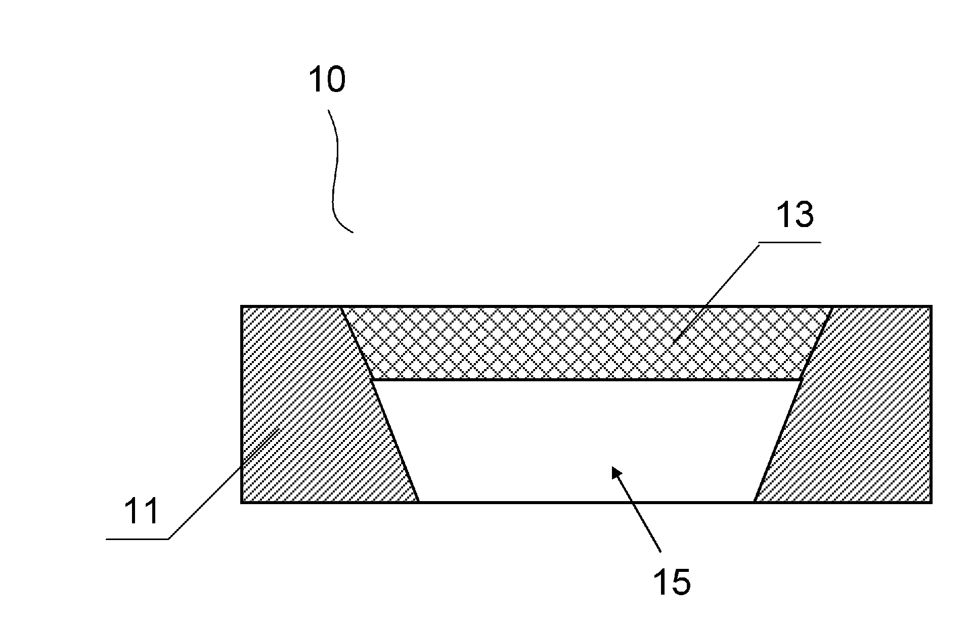
[0042] Herein, the "front side" of the wafer refers to the side where the sensing film is located, and the "back side" of the wafer refers to the side opposite to the "fr...
PUM
| Property | Measurement | Unit |
|---|---|---|
| thickness | aaaaa | aaaaa |
| diameter | aaaaa | aaaaa |
Abstract
Description
Claims
Application Information