
Micro assembly process for millimeter-wave circuit

A micro-assembly and millimeter-wave technology, applied in the direction of high-frequency amplifiers, etc., can solve the problems of not being able to play the performance of the MMIC chip, damaging the chip, and having no information to consult and learn from.

Active Publication Date: 2012-10-31
SHENZHEN TONGCHUANG COMM
View PDF3 Cites 9 Cited by
  • Summary
  • Abstract
  • Description
  • Claims
  • Application Information

AI Technical Summary

Problems solved by technology

If the installation process is wrong, the performance of the MMIC chip will not be fully utilized, and the chip will be damaged if it is serious.
Foreign countries have always been in the leading position in the manufacture, installation and use of MMIC chips, but they are in a state of technical secrecy in terms of millimeter-wave micro-assembly technology, and there is no complete information to consult and learn from.

Method used


Image

  • Micro assembly process for millimeter-wave circuit
  • Micro assembly process for millimeter-wave circuit
  • Micro assembly process for millimeter-wave circuit

Examples


Embodiment Construction

[0034] In order to make the object, technical solution and advantages of the present invention clearer, the present invention will be further described in detail below in conjunction with the accompanying drawings and embodiments. It should be understood that the specific embodiments described here are only used to explain the present invention, not to limit the present invention.

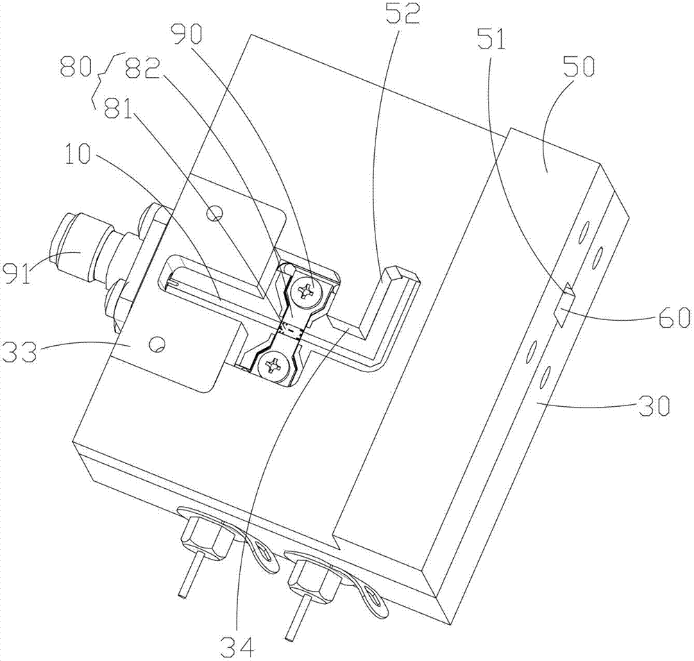
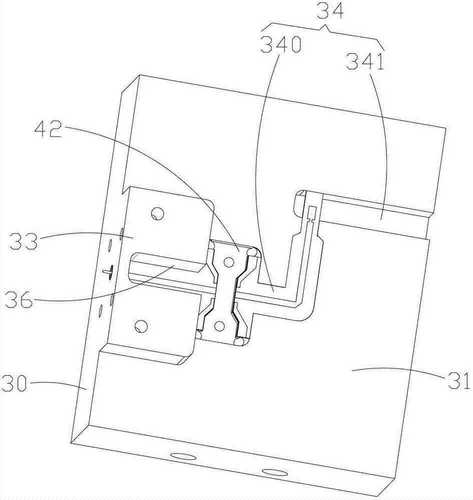
[0035] Please also see Figure 1 to Figure 9 , the implementation of the millimeter-wave circuit micro-assembly process provided by the embodiment of the present invention is equipped with a dust-free studio with a cleanliness of 100,000. All personnel entering the clean room must wear anti-static dust-proof clothing and anti-static shoes. . All personnel must wear anti-static bracelets as long as they come into contact with the circuit.

[0036] The millimeter-wave circuit micro-assembly process of the present invention is equipped with a gold wire pressure welding machine, a eutectic soldering ...


PUM


Abstract

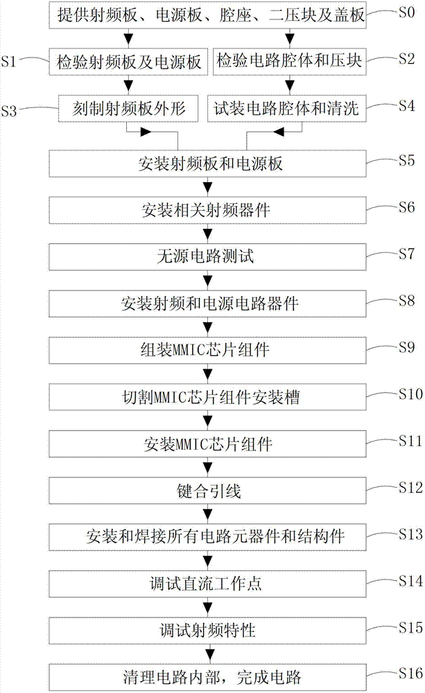
The invention provides a micro assembly process for a millimeter-wave circuit. The process comprises the following steps: providing an RF board, a power board, a cavity seat, two pressure blocks and a cover plate; detecting the RF board and the power board, as well as a circuit cavity body and the two pressure blocks; engraving the RF board shape; carrying out trail assembly of the circuit cavity body, and then cleaning; installing the RF board and the power board, as well as related RF devices; testing a passive circuit; installing RF and power circuit devices; assembling MMIC (Monolithic Microwave Integrated Circuit) chip components; forming installation grooves of the MMIC chip components; installing the MMIC chip components in the grooves; bonding lead wires; installing and welding circuit devices and structural parts; debugging DC working points and the RF characteristics of the circuit; and cleaning the interior of the circuit. Due to the adoption of the process, the MMIC chip can be effectively installed and used, accordingly, the functions of the MMIC chip can played, so as to improve the success rate of manufacturing the microwave millimeter wave circuit and a subsystem through utilizing the MMIC chip; and in addition, the blank in millimeter-wave micro assembly technology is filled in China.

Description

technical field [0001] The invention belongs to the technical field of millimeter-wave circuits, and in particular relates to a micro-assembly process for millimeter-wave circuits. Background technique [0002] Millimeter wave circuit technology is used in communication, telemetry and remote sensing, and radar, and has a wide range of applications and requirements in civil, military, and deep space exploration. With the development of modern process technology and semiconductor technology, MMIC (monolithic microwave integrated circuit) chips have widely replaced traditional microwave hybrid integrated circuits composed of discrete devices, and their performance is far superior to hybrid integrated circuits. In recent years, with the increasing demand of the military and civilian communication market, the output power of MMIC power amplifiers is getting higher and higher, and the operating frequency is getting higher and higher. [0003] The MMIC chip uses a piece of compoun...

Claims


Application Information

Patent Timeline
Patent Type & Authority Applications(China)
IPC IPC(8): H03F3/189
Inventor 侯世淳彭利利李云峰
Owner SHENZHEN TONGCHUANG COMM
Learn More