Color filter array substrate and manufacturing method thereof

A color filter array and color filter technology, applied in semiconductor/solid-state device manufacturing, optics, nonlinear optics, etc., can solve the problems of electrostatic discharge of display panels, unfavorable transparent conductive layers, deposition, etc., to avoid electrostatic discharge. Effect

Active Publication Date: 2012-11-07
TCL CHINA STAR OPTOELECTRONICS TECH CO LTD
View PDF10 Cites 7 Cited by
  • Summary
  • Abstract
  • Description
  • Claims
  • Application Information

AI Technical Summary

Problems solved by technology

However, in order to ensure the display effect of the liquid crystal panel, the thickness of the color filter is about ten times the thickness of the drain of the thin film transistor, and the height difference between the two will make the inclination angle of the side wall of the opening approach 90 degrees. It is not conducive to the deposition of the transparent conductive layer on the opening, and it may also cause the risk of electrostatic discharge (Electro Static Discharge, ESD) in the liquid crystal display panel

Method used


Image

  • Color filter array substrate and manufacturing method thereof
  • Color filter array substrate and manufacturing method thereof
  • Color filter array substrate and manufacturing method thereof

Examples


Embodiment Construction

[0029] The following descriptions of the various embodiments refer to the accompanying drawings to illustrate specific embodiments in which the present invention can be practiced. The directional terms mentioned in the present invention, such as "up", "down", "front", "back", "left", "right", "top", "bottom", "horizontal", "vertical", etc. , are for orientation only with reference to the attached drawings. Therefore, the directional terms used are used to illustrate and understand the present invention, but not to limit the present invention.

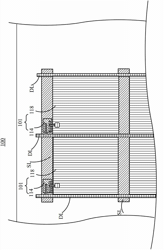
[0030] see figure 1 , figure 1 is a schematic diagram of a liquid crystal display panel 100 according to an embodiment of the present invention. The liquid crystal display panel 100 includes a plurality of pixel units 101 , a plurality of scan lines SL and a plurality of data lines DL. Each pixel unit 101 includes a thin film transistor 114 and a pixel electrode 118 . Each thin film transistor 114 is electrically connected to a pix...


PUM


Abstract

The invention discloses a color filter array substrate and a manufacturing method thereof. The color filter array substrate comprises a transparent substrate, a thin film transistor, a color filter unit and a pixel electrode, wherein the color filter unit is positioned on a groove of the transparent substrate and is used for converting light rays entering the color filter unit into light rays with a preset color; the pixel electrode is positioned on the color filter unit, coupled to the drain of the thin film transistor and used for controlling the liquid crystal rotating direction of a liquid crystal layer according to the level of an electric signal transmitted to the drain when the grid of the thin film transistor receives scanning impulse. The color filter unit is formed on a first groove, the pixel electrode is formed on the color filter unit, and an opening for connecting the drain of the thin film transistor with the pixel electrode is not required to be formed on a protective layer; and therefore, the etching process of forming the opening on the protective layer can be eliminated.

Description

technical field [0001] The invention relates to a liquid crystal display panel and a manufacturing method thereof, in particular to a color filter array substrate and a manufacturing method thereof. Background technique [0002] Displays with advanced functions have gradually become an important feature of today's consumer electronics products. Liquid crystal displays have gradually become widely used in various electronic devices such as mobile phones, personal digital assistants (PDAs), digital cameras, computer screens or laptop screens with high resolution. rate color screen monitor. [0003] A traditional liquid crystal display panel is composed of a color filter substrate (color filter), a thin film transistor array substrate (thin film transistor array substrate, TFT array substrate), and a liquid crystal layer (liquid crystal layer) disposed between the two substrates. constitute. However, the resolution of this liquid crystal display panel is poor, the aperture r...

Claims


Application Information

Patent Timeline
IPC IPC(8): G02F1/1335G02F1/1343G02F1/1362H01L21/77H01L27/12
CPCH01L29/786G02F2001/136222G02F1/1368G02F1/134309G02F1/136204G02F1/136222H01L27/1218
Inventor 赵小虎
Owner TCL CHINA STAR OPTOELECTRONICS TECH CO LTD
Why Eureka
Try Eureka