Method for preparing TM-SOI (Thick-Membrane Silicon-On-Insulator) silicon chip
A TM-SOI, silicon wafer technology, applied in the field of thick film TM-SOI silicon wafer preparation, can solve the problems of uneven thickness of SOI top layer silicon film, poor CMP uniformity control ability, etc. The effect of fewer defects and lower roughness
- Summary
- Abstract
- Description
- Claims
- Application Information
AI Technical Summary
Problems solved by technology
Method used
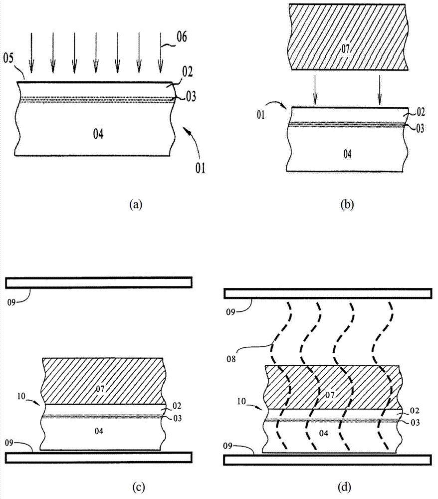
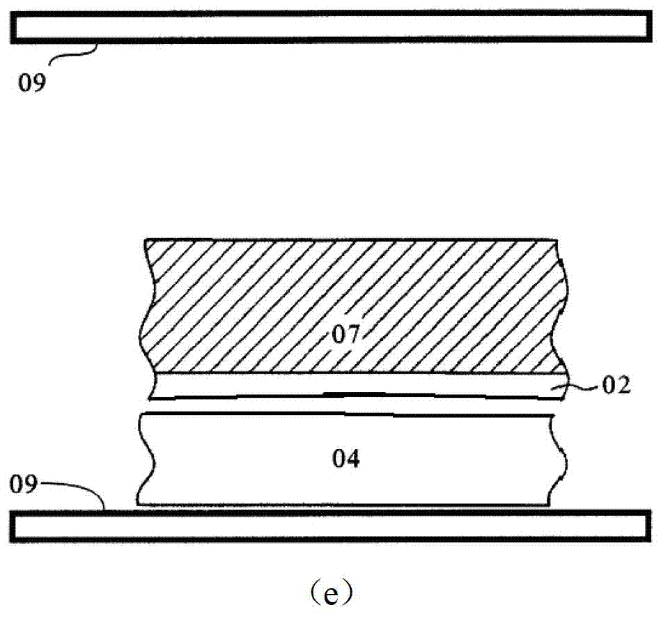
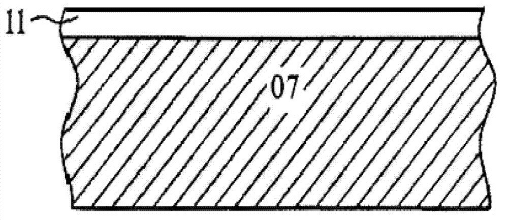
Image

Examples
Embodiment 1
[0065] The original silicon wafer is P-type, the lattice direction is (100), the resistance value is 10-50ohm / cm, and the surface coverage Silicon dioxide (SiO2), polished on one side, 8 pieces of 8" silicon wafers, the dose is 4.0×10 16 / cm 2 , the implantation energy is 200KeV, hydrogen molecular ions (H 2 + )injection. The substrate silicon wafer is P-type, the lattice direction is (100), the resistivity is 0.010-0.020ohm-cm, and the silicon wafer is polished on one side. Two silicon wafers were bonded into a bonded structure by plasma-enhanced bonding at room temperature, placed in a commercially adjustable temperature microwave oven, and annealed at a transition temperature of 200°C for 15 minutes, and then immediately at this temperature After 15 minutes of microwave irradiation at 2.45GHz frequency and 1000W output power, the film with an average thickness of 0.6452 μm was peeled off to form an SOI wafer material.
[0066] Take 6 pieces of SOI wafer materials prep...
Embodiment 2
[0075] Take 3 pieces of SOI wafer material after CMP treatment formed by the TM-SOI technology in Example 1, place them in the reaction chamber of the epitaxial furnace, raise the temperature to 1130 ° C, pass 80 slm of hydrogen, and bake the surface to remove oxidation layer. Heating to 1200° C., introducing 3 slm of HCl for chemical vapor polishing. After 5s, blow air to remove impurities and HCl, then cool down to 1130°C, and feed 3g / min SiHCl under normal pressure 3 , 50sccm B 2 h 6 , for 300s deposition. Finally, stop passing SiHCl 3 , B 2 h 6 , blowing hydrogen to remove SiHCl 3 , B 2 h 6 , cooled to room temperature, blown away the hydrogen, flushed with nitrogen again, and took out the silicon wafer. Table 3 is the test data:
[0076] table 3
[0077]
[0078] From Table 3, it can be seen that the parameters such as TTV and RMS are significantly better than those of the CMP method, and the SOI formed by the CMP method cannot reach the thickness of the top ...
PUM
| Property | Measurement | Unit |
|---|---|---|
| thickness | aaaaa | aaaaa |
Abstract
Description
Claims
Application Information
 - R&D Engineer
- R&D Manager
- IP Professional
- Industry Leading Data Capabilities
- Powerful AI technology
- Patent DNA Extraction
Browse by: Latest US Patents, China's latest patents, Technical Efficacy Thesaurus, Application Domain, Technology Topic.
© 2024 PatSnap. All rights reserved.Legal|Privacy policy|Modern Slavery Act Transparency Statement|Sitemap