Method for generating test graph for detecting decoding circuit of memory

A technology of decoding circuits and test patterns, which is applied in the direction of measuring electricity, measuring electrical variables, instruments, etc., can solve the problem that the test method does not have universality, and achieve the effect of saving test costs

Active Publication Date: 2012-11-28
SHANGHAI FUDAN MICROELECTRONICS GROUP
View PDF7 Cites 0 Cited by
  • Summary
  • Abstract
  • Description
  • Claims
  • Application Information

AI Technical Summary

Problems solved by technology

Therefore, the diagonal test method is not universal

Method used


Image

  • Method for generating test graph for detecting decoding circuit of memory
  • Method for generating test graph for detecting decoding circuit of memory
  • Method for generating test graph for detecting decoding circuit of memory

Examples


Embodiment 1

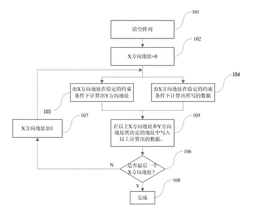
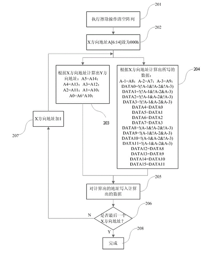
[0040] The full address of a NOR FLASH memory storage array is A[0:14]; the address of the decoding circuit in the X direction is A[6:14], and 512 WORDLINEs are decoded; the address of the decoding circuit in the Y direction is A[0 :5], 64 WORDs are decoded, and each WORD has a bit width of 16 bits, so there are 64*16=1024 BITLINEs in total. The storage array can be divided into two square arrays (each array is 512*512), the data DATA0~DATA3 and DATA7~DATA10 are located in the square array A, and the data DATA4~DATA7 and DATA8~DATA15 are located in the square array array B. The schematic diagram of the array address is as follows Figure 5 shown. If the array is erased, all BITs are in a 1 state; if a BIT is selected for programming, it is in a 0 state. The principle of generating the checkerboard test pattern is that when A0^A6^A10=0 (^ means XOR), the WORD will be programmed with the data of 0000h, otherwise the WORD will remain in the erased state of FFFFh.

[0041] The...

Embodiment 2

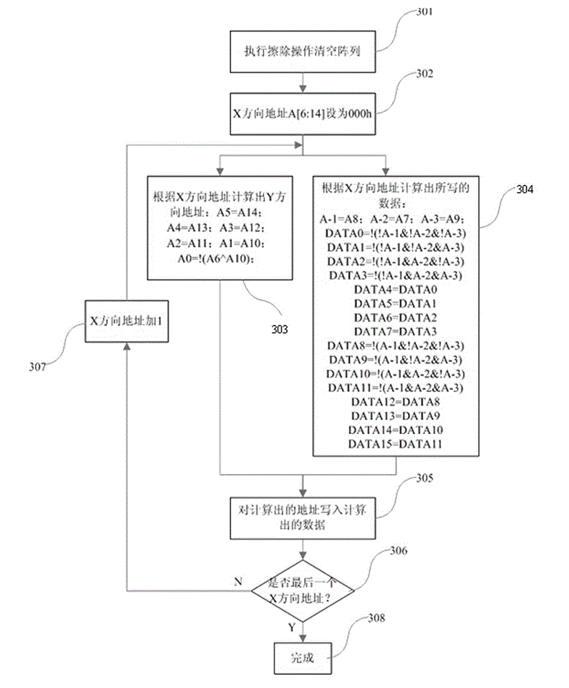
[0074] Embodiment 2: the full address of a NOR FLASH memory storage array is A[0:14]; the address of the decoding circuit in the X direction is A[6:14], and 512 WORDLINEs are decoded; the address of the decoding circuit in the Y direction It is A[0:5], 64 WORDs are decoded, and each WORD has a bit width of 16 bits, so there are 64*16=1024 BITLINEs in total. The storage array can be divided into two square arrays (each array is 512*512), the data DATA0~DATA3 and DATA7~DATA10 are located in the square array A, and the data DATA4~DATA7 and DATA8~DATA15 are located in the square array array B. The schematic diagram of the array address is as follows Figure 5 shown. If the array is erased, all BITs are in a 1 state; if a BIT is selected for programming, it is in a 0 state. The principle of generating the test pattern of the reverse checkerboard is that when A0^A6^A10=1 (^ means XOR), the WORD will be programmed with the data of 0000h, otherwise the WORD will remain in the erase...


PUM


Abstract

The invention discloses a method for generating a test graph for detecting a decoding circuit of a memory. The method comprises the following steps of: emptying an array; initializing an X direction address; under a given constraint condition, calculating a Y direction address according to the X direction address, and calculating data to be written; and finally, writing the obtained data into an address determined by the X direction address and the Y direction address obtained in the step 103, and traversing the X direction address, and repeating the operation. The method is used for detecting whether the decoding circuit in the memory is normal and is universal, so that the test graph for detecting the decoding circuit can be generated by the method according to different memories, and the test graph of the decoding circuit can be compatible with other test graphs; and an array emptying operation for writing between two test graphs is eliminated, so that the test cost is saved.

Description

technical field [0001] The invention relates to a method for generating a test pattern for detecting a memory decoding circuit. Background technique [0002] Existing test pattern data for non-volatile memory circuits such as FLASH memory mainly includes all 0s, all 1s, checkerboard data, diagonal data and some other data such as 5555, AAAA, etc. Among them, the diagonal data can be used to detect the decoding circuit of the memory, and can be used to detect the over-erasing problem of the NOR flash memory (NOR FLASH). But to write the graph data of the diagonal, must require the tester to fully understand the architecture of the memory array. Moreover, for testers, different products have different internal architectures, and the corresponding relationship between the physical location and address of each BIT in the storage array is also different. It is necessary to develop vectors separately to generate corresponding diagonal data. Therefore, the diagonal test method is...

Claims


Application Information

Patent Timeline
Patent Type & Authority Applications(China)
IPC IPC(8): G01R31/3183
Inventor 董艺周军刘剑海
Owner SHANGHAI FUDAN MICROELECTRONICS GROUP
Why Eureka
Try Eureka