LED lamp strip structure and manufacturing method thereof

A technology of LED light bar and manufacturing method, which is applied in the direction of lighting and heating equipment, electrical components, circuits, etc., and can solve the problems of chromatic aberration, large chromatic aberration, and large light emitting surface of light emitting diode packaging structure

Inactive Publication Date: 2012-12-05
ZHANJING TECH SHENZHEN +1
View PDF4 Cites 5 Cited by
  • Summary
  • Abstract
  • Description
  • Claims
  • Application Information

AI Technical Summary

Problems solved by technology

When a fluorescent layer is formed on the surface of the encapsulating colloid, due to the different light intensities at different light emitting positions, for example, the light intensity directly above the light-emitting diode is higher, and the light intensity at the position deviated from directly above is lower, resulting in different light emitting positions. Different conversion ratios lead to chromatic aberration in the final output of the li

Method used


Image

  • LED lamp strip structure and manufacturing method thereof
  • LED lamp strip structure and manufacturing method thereof
  • LED lamp strip structure and manufacturing method thereof

Examples


Embodiment Construction

[0017] The present invention will be further described in detail below in conjunction with the accompanying drawings.

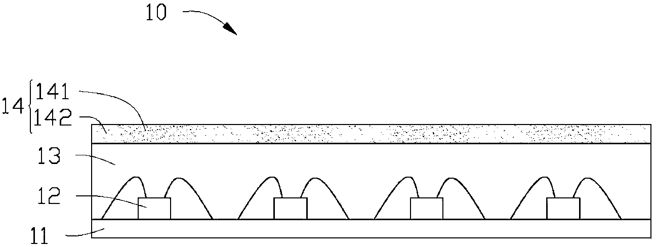
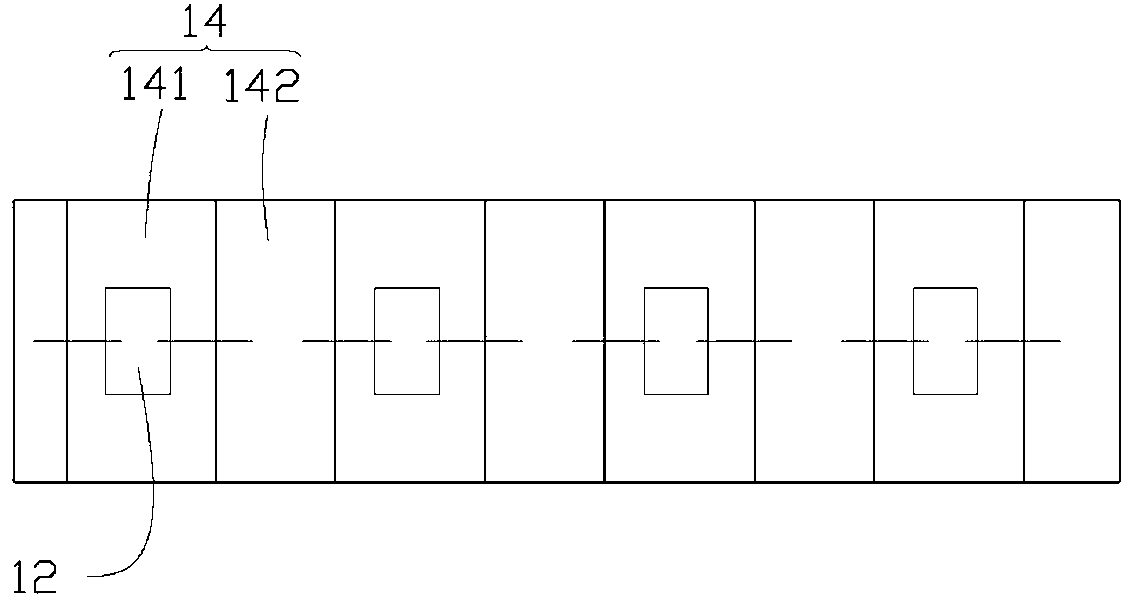
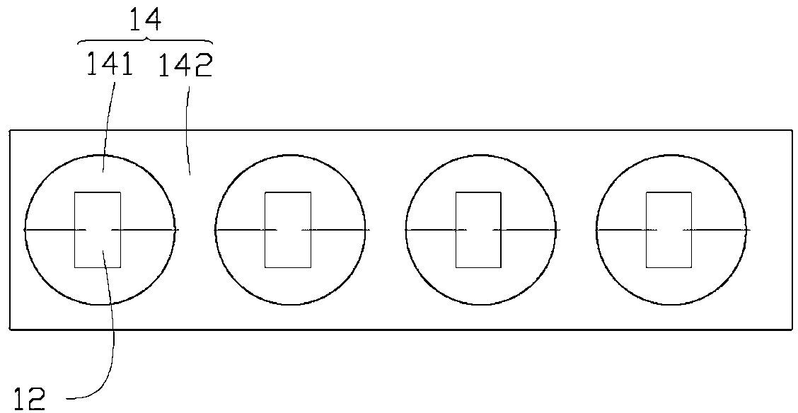
[0018] see figure 1 , An LED light bar structure 10 provided in an embodiment of the present invention includes a substrate 11 , a light emitting diode chip 12 , a package body 13 and a fluorescent layer 14 .

[0019] The substrate 11 is used to support the LED chip 12 , the packaging body 13 and the fluorescent layer 14 thereon. The substrate 11 is in the shape of a flat plate, which is a circuit board with a metal substrate. During specific implementation, several grooves may be formed on the upper surface of the substrate 11 for placing the light emitting diode chips 12 .

[0020] The light emitting diode chip 12 is fixed on the upper surface of the substrate 11 by adhesive and electrically connected to the circuit on the substrate 11 by wire bonding. It can be understood that the LED chip 12 can also be electrically fixed on the substrate 11 by flip-ch...


PUM


Abstract

An LED lamp strip structure comprises a substrate, a plurality of light emitting diode chips arranged on the substrate, and a fluorescent layer enclosing the light emitting diode chips. The fluorescent layer comprises a plurality of first portions and a plurality of second portions, wherein the first portions are arranged right above the light emitting diode chips, and the second portions are connected between every two adjacent first portions. The concentration of fluorescent powder inside the first portions is higher than that of the fluorescent powder in the second portions. The invention further relates to a manufacturing method of the LED lamp strip structure.

Description

technical field [0001] The invention relates to a semiconductor structure, in particular to an LED light bar structure and a manufacturing method thereof. Background technique [0002] In the current packaging structure of light-emitting diodes, fluorescent materials are often doped inside the packaging colloid or a fluorescent layer is formed on the surface of the packaging colloid. The light emitted by the light-emitting diodes excites different fluorescent materials to emit light, thereby obtaining light of the desired color. When a fluorescent layer is formed on the surface of the encapsulating colloid, due to the different light intensities at different light emitting positions, for example, the light intensity directly above the light-emitting diode is higher, and the light intensity at the position deviated from the directly above is lower, resulting in different light emitting positions. The different conversion ratios lead to chromatic aberration in the final output...

Claims


Application Information

Patent Timeline
IPC IPC(8): F21S4/00F21V19/00F21V9/10F21Y101/02F21K9/90F21V9/40F21Y103/10F21Y115/10
CPCH01L2224/48091
Inventor 张耀祖
Owner ZHANJING TECH SHENZHEN
Why Eureka
Try Eureka