
A strip of a contactless large chip smart card
A large chip and smart card technology, which is applied to recording carriers, instruments, and electrical components used in machines, can solve problems such as poor tensile strength, cumbersome processes, and increased costs, and achieve the effect of maximizing area utilization
Patent Information
- Authority / Receiving Office
- CN · China
- Patent Type
- Patents(China)
- Current Assignee / Owner
- Publication Date
- 2015-09-30
Smart Images
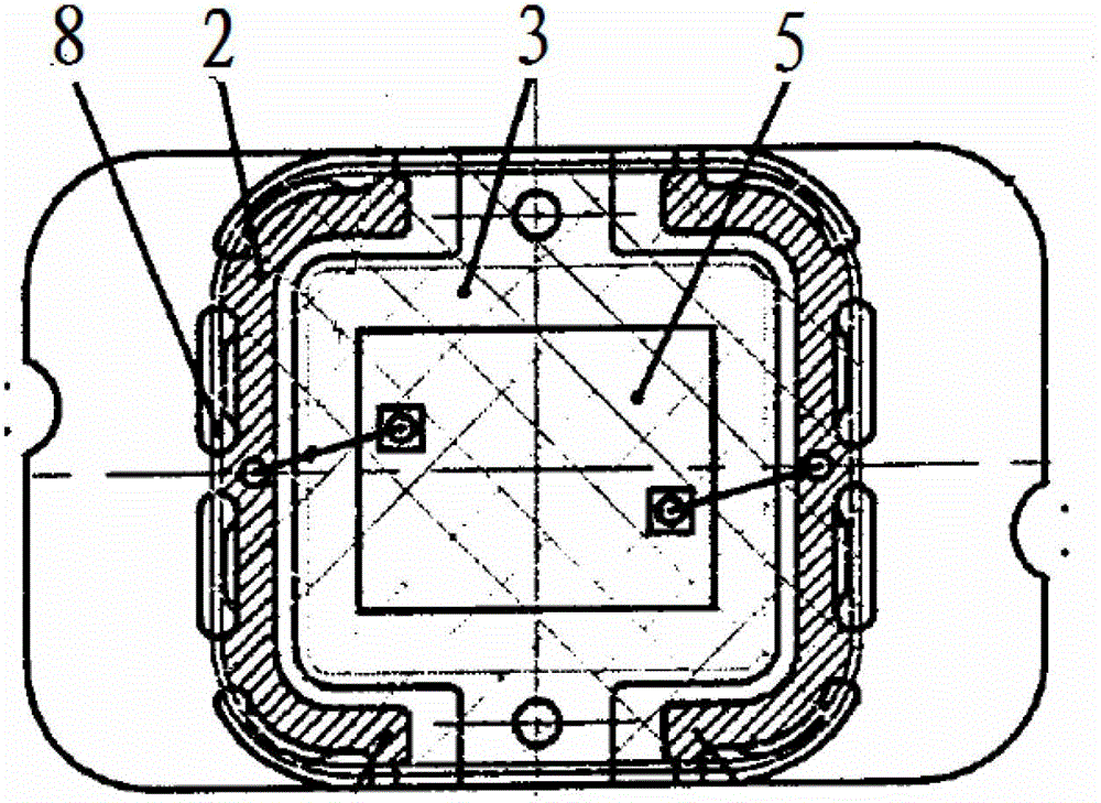
Figure 1 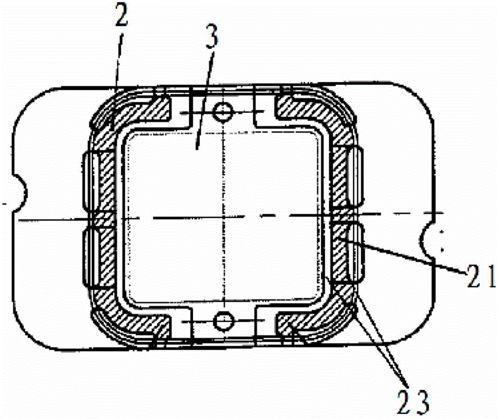
Figure 2 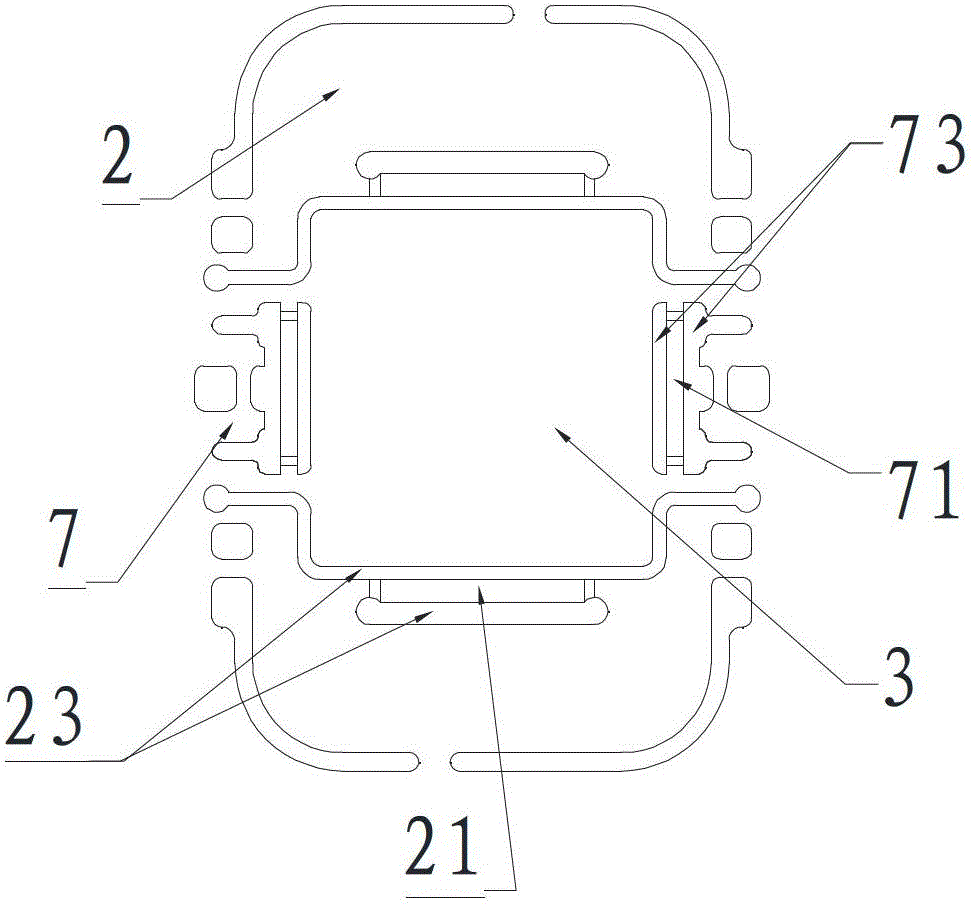
Figure 3
Abstract
Description
technical field
[0001] The invention relates to the field of microelectronic semiconductor packaging, in particular to a strip of a non-contact large-chip smart card. Background technique
[0002] Contactless smart cards have been widely used in second-generation ID cards, public transportation cards and campus cards. There is a module on the contactless smart card, which is packaged on the strip by single-sided molding process. The total package height of the module is generally below 0.4 mm (0.33 mm is currently used in large quantities, and 0.25 mm is being developed. total package height of the module).
[0003] see figure 1 The strip of the early contactless smart card module includes a chip bonding cavity 3 arranged in the central area of the strip, and the chip 5 is fixed in the chip bonding cavity 3 by fast curing epoxy resin. Lead contact pieces 2 are arranged around the outer periphery of the die bonding cavity 3 . The chip 5 is encapsulated by a molded body ...
Examples
Embodiment Construction
[0025] see Figure 3 to Figure 10 , the inventor of the present invention, in order to better understand the technical solution of the present invention, the following will be described in detail through specific embodiments and in conjunction with the accompanying drawings.
[0026] 1. The first embodiment
[0027] Figure 3 to Figure 6 Shown is a first embodiment of a strip for a contactless large chip smart card of the present invention. In the first embodiment, the strip includes: a chip bonding cavity 3 arranged in the central area of the strip, two lead contact pieces 2 respectively located on opposite sides of the chip bonding cavity 3, and two lead contact pieces 2 respectively located on the chip bonding cavity 3 Weld the sprue bottom plate 7 on both sides of the cavity 3 .
[0028] The two sides 23 of each lead wire contact piece 2 are hollowed out, and the middle of the two sides 23 is an upward protrusion 21, so that the described lead wire contact piece 2 has...