Interface layer treatment method for TFT (thin film transistor) dry etching process

An interface layer and process technology, applied in the field of dry engraving process, can solve the problems of long cycle, high cost, affecting the company's production capacity, etc., to achieve the effect of strengthening processing, increasing uniformity and improving uniformity

Inactive Publication Date: 2012-12-12
SHANGHAI ADVANCED RES INST CHINESE ACADEMY OF SCI
View PDF3 Cites 3 Cited by
  • Summary
  • Abstract
  • Description
  • Claims
  • Application Information

AI Technical Summary

Problems solved by technology

However, the disadvantages of retrofitting equipment are: the cost of retrofitting is high and the period is long; in addition, changes in the hardware structure of equip

Method used


Image

  • Interface layer treatment method for TFT (thin film transistor) dry etching process

Examples


Embodiment 1

[0019] The adjustment of the interface pretreatment is: the RF power is increased from 3200w to 4000w, the cavity pressure is adjusted from 12Pa to 9Pa, and the mixed gas includes SF 6 (80SCCM, standard milliliters per minute), He (400SCCM, standard milliliters per minute), O 2 (800SCCM, standard milliliters per minute), the entire pretreatment time is 18 seconds.

[0020] The results show that after the improved pretreatment conditions, the etching uniformity changed from 21.5% to 11.3%

Embodiment 2

[0022] The adjustment of the interface pretreatment is as follows: the RF power is increased from 3200w to 4500w, the cavity pressure is adjusted from 12Pa to 8Pa, and the mixed gas includes SF 6 (80SCCM, standard milliliters per minute), He (400SCCM, standard milliliters per minute), O 2 (800SCCM, standard milliliters per minute), the entire pretreatment time is 18 seconds.

[0023] The results show that after the improved pretreatment conditions, the etching uniformity changed from 21.5% to 10.1%

Embodiment 3

[0025] The adjustment of the interface pretreatment is as follows: the RF power is increased from 3200w to 5000w, the cavity pressure is adjusted from 12Pa to 6Pa, and the mixed gas includes SF 6 (80SCCM, standard milliliters per minute), He (400SCCM, standard milliliters per minute), O 2 (800SCCM, standard milliliters per minute), the entire pretreatment time is 18 seconds.

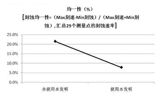
[0026] The results show that after the improved pretreatment conditions, the etching uniformity changed from 21.5% to 7.8%. The results are shown in figure 1 shown.


PUM


Abstract

Disclosed is an interface layer treatment method for a TFT (thin film transistor) dry etching process. According to the method, the RF (radio frequency) power is increased to 4000w-5000w from 3200w, the pressure of a cavity is adjusted to 6Pa-9Pa from 12Pa, and mixed gas consists of 100 standard milliliters of SF6 per minute, 500 standard milliliters of He per minute and 800 standard milliliters of O2 per minute. By adjusting RF parameters and pressure parameters of the mixed gas, an interface layer can be uniformly removed, so that the uniformity of an a-Si layer etched in a follow-up step is improved.

Description

technical field [0001] The present invention relates to a semiconductor process, in particular to a dry etching process in a thin film transistor (hereinafter referred to as TFT) manufacturing method. Background technique [0002] The TFT-LCD Array (Thin Film Transistor Liquid Crystal Display Array) process is the front process of the liquid crystal display module. It is used to form an electrical switch on the glass substrate to control whether the light emitted by the backlight can pass through. The substrate process structure is similar to that of a semiconductor. The dry etching (Dry Etching) technology is a technology commonly used in the manufacture of (Thin film transistor, thin film transistor) TFT-LCD (Liquid crystal display, liquid crystal display) to etch non-metallic films, such as SiNx, a-Si Wait. Usually, in the manufacturing process of 4Mask array thin film transistors, after the amorphous silicon (a-Si) film is formed, a metal layer such as Cr, Mo / Al, etc. w...

Claims


Application Information

Patent Timeline
IPC IPC(8): H01L21/3213H01L21/77
Inventor 张其国于涛郭晓东申剑锋
Owner SHANGHAI ADVANCED RES INST CHINESE ACADEMY OF SCI
Why Eureka
Try Eureka