
Balanced dual-pass band filter

A dual-passband filter and balanced technology, applied in waveguide devices, electrical components, circuits, etc., can solve the problems of complexity, design difficulty, narrow bandwidth of the first passband, etc., and achieve high common-mode rejection Effect

Inactive Publication Date: 2012-12-12
NANTONG UNIVERSITY
View PDF0 Cites 16 Cited by
  • Summary
  • Abstract
  • Description
  • Claims
  • Application Information

AI Technical Summary

Problems solved by technology

Ultra-wideband common-mode rejection is still difficult to achieve, and the general common-mode rejection method needs to load lumped elements or microstrip stubs, which will make the design difficult and complicated
On the other hand, the existing balanced dual-passband filter has a relatively narrow bandwidth of the first passband (range <30%)
At present, there is no clear solution to design a balanced dual-passband filter that can independently control the two passbands and have a wide first passband and ultra-wideband common-mode rejection.

Method used


Image

  • Balanced dual-pass band filter
  • Balanced dual-pass band filter
  • Balanced dual-pass band filter

Examples


Embodiment Construction

[0026] The present invention will be further explained below in conjunction with the embodiments and accompanying drawings.

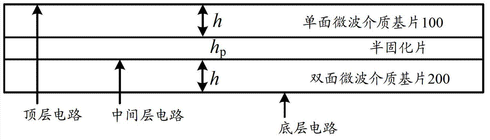
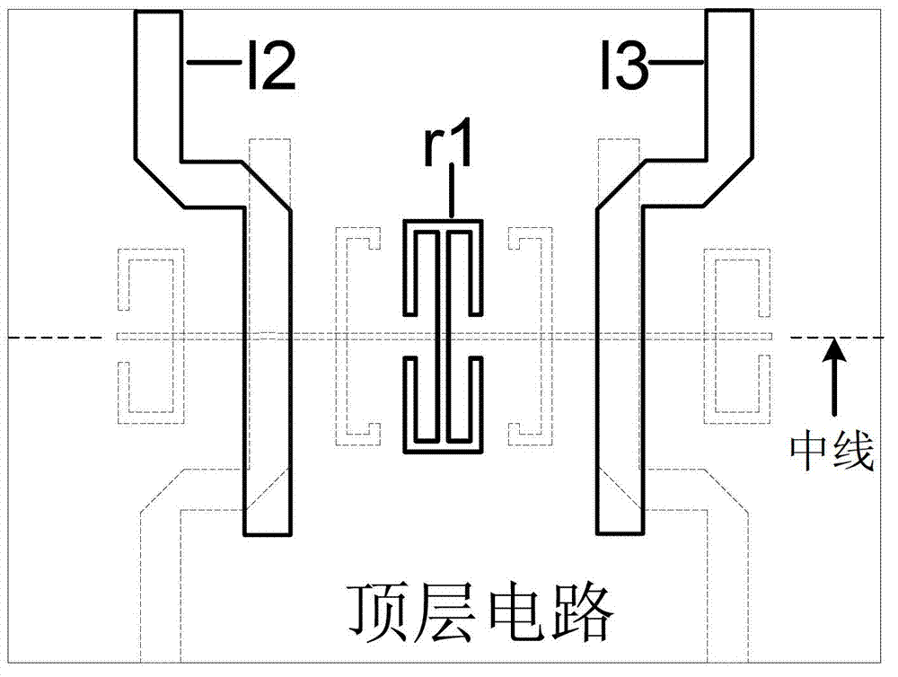
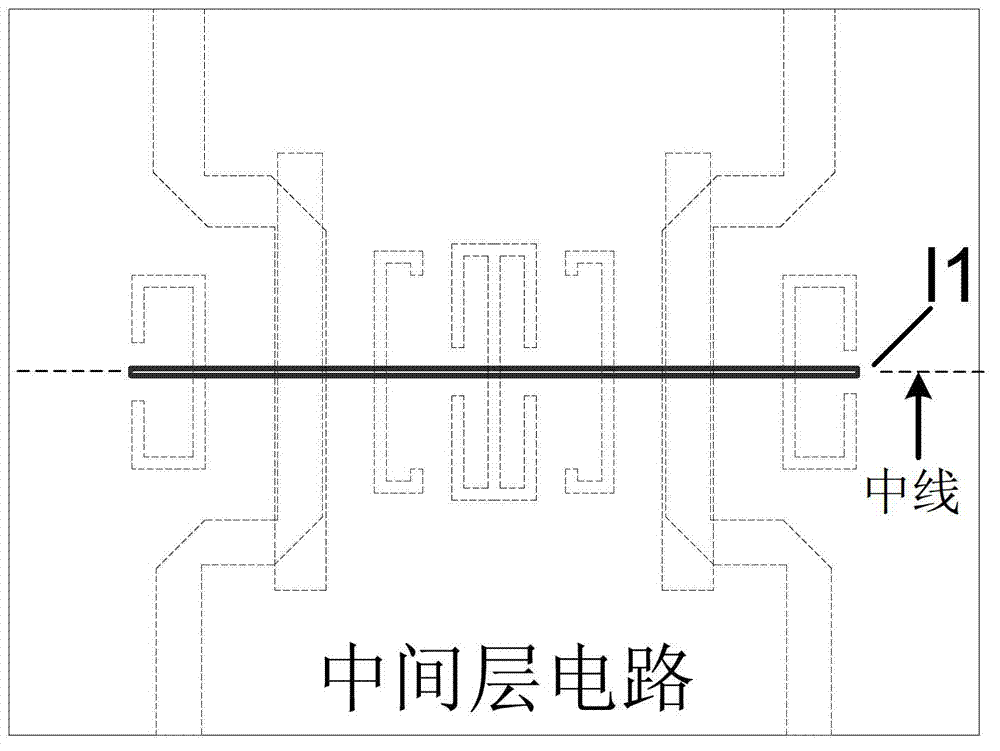
[0027] see Figure 1-2C , the balanced double-passband filter of the present invention includes a single-sided microwave dielectric substrate 100 and a double-sided microwave dielectric substrate 200 that are correspondingly arranged and connected. Wherein, the metal surface of the double-sided microwave dielectric substrate 200 facing the single-sided microwave dielectric substrate 100 is a common ground, and a groove line l1 is arranged at the center line of the metal surface. A first microstrip transmission line l2 and a second microstrip transmission line l3 perpendicular to the slot line l1 are arranged symmetrically on the metal surface of the single-sided microwave dielectric substrate 100 . The metal surface of the double-sided microwave dielectric substrate 200 facing away from the single-sided microwave dielectric substrate 100 is provided wi...


PUM


Abstract

The invention discloses a balanced dual-pass band filter which comprises a three-layer circuit structure consisting of a single face microwave dielectric substrate and a double face microwave dielectric substrate. A slot line is arranged in a middle line of a metal face between the single face microwave dielectric substrate and the double face microwave dielectric substrate. The single face microwave dielectric substrate is symmetrically provided with a first microstrip transmission line and a second microstrip transmission line. The double face microwave dielectric substrate is provided with a third microstrip transmission line and a fourth microstrip transmission line symmetrically distributed with the first and second microstrip transmission lines in relation to the slot line. The single or double face microwave dielectric substrate is further provided with a first resonator, and a second resonator, a third resonator as well as a fourth resonator and a fifth resonator symmetrically distributed inside and outside the third and fourth microstrip transmission lines in relation to the first resonator, respectively. Common mode rejection is formed through transition from the balanced microstrip line to the slot line, the frequency of a first pass band is adjusted by controlling the length of two pairs of the microstrip lines and the slot lines, and the frequency of a second pass band is controlled by controlling the size of the second and third resonators.

Description

technical field [0001] The invention relates to the field of microwave communication, in particular to a balanced double-passband filter. Background technique [0002] Over the years, balanced filters have gained more and more importance in modern communication systems due to their ability to suppress interference such as noise, crosstalk, and inter-component interference compared to single-ended filters. Ability. Moreover, balanced filters do not require a balanced-to-unbalanced converter (balun) and can be directly connected to other balanced circuits. Balanced dual-passband filter is an important member of balanced filters. Various design methods have been studied at home and abroad, such as: two pairs of balanced resonators, cross-coupled mid-loaded half-wavelength resonators, mid-range End-loaded step impedance resonators and coupled step impedance resonators. But none of these design methods involve designing balanced filters using balanced microstrip-to-slot transi...

Claims


Application Information

Patent Timeline
IPC IPC(8): H01P1/203
Inventor 施金陈建新包志华周立衡唐慧杨永杰陆清源
Owner NANTONG UNIVERSITY
Learn More