Manufacturing method of semiconductor device

A manufacturing method and semiconductor technology, applied in the fields of semiconductor/solid-state device manufacturing, semiconductor devices, electrical components, etc., can solve the problems of increased design pattern density, micro-loading effect, and decreased etching rate, so as to improve etching efficiency, reduce The effect of the micro-loading effect

Active Publication Date: 2015-07-08
SEMICON MFG INT (SHANGHAI) CORP
View PDF3 Cites 0 Cited by
  • Summary
  • Abstract
  • Description
  • Claims
  • Application Information

AI Technical Summary

Problems solved by technology

Due to the increase in device design pattern density due to device scaling, the anisotropic wet etch followed by the dry etch process can cause microloading effects, resulting in reduced etch rates and poorer etch performance

Method used


Image

  • Manufacturing method of semiconductor device
  • Manufacturing method of semiconductor device
  • Manufacturing method of semiconductor device

Examples


Embodiment Construction

[0024] In the following description, numerous specific details are set forth in order to provide a more thorough understanding of the present invention. It will be apparent, however, to one skilled in the art that the present invention may be practiced without one or more of these details. In other instances, some technical features known in the art have not been described in order to avoid obscuring the present invention.

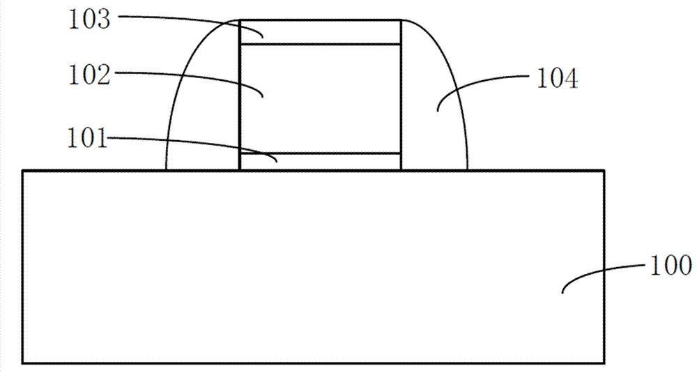
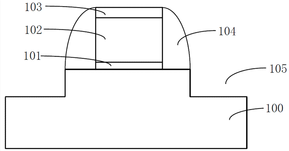
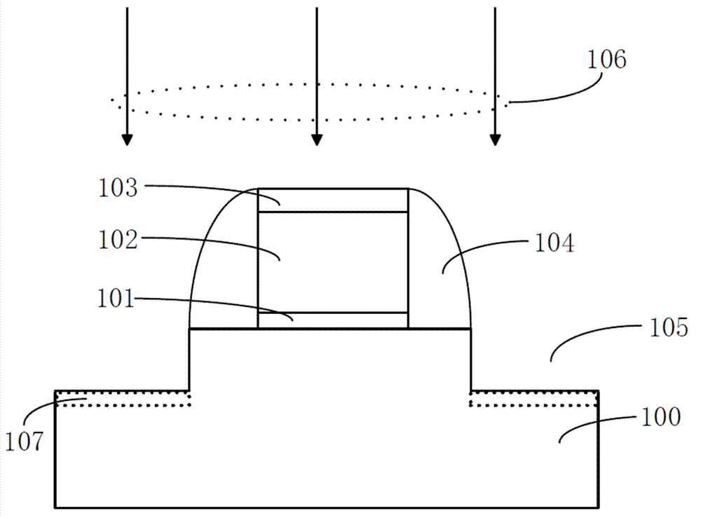
[0025] In order to thoroughly understand the present invention, detailed steps will be presented in the following description to explain how the present invention forms a Σ-shaped groove for embedded SiGe strained MOS devices. Obviously, the practice of the present invention is not limited to the specific details familiar to those skilled in the semiconductor arts. Preferred embodiments of the present invention are described in detail below, however, the present invention may have other embodiments in addition to these detailed descriptions.

[0026] It ...


PUM


Abstract

The invention provides a manufacturing method of a semiconductor device. The manufacturing method comprises the following steps: providing a semiconductor substrate and forming a gate structure on the semiconductor substrate; forming a groove at a part which is prone to formation of a source region / drain region in the semiconductor substrate; performing pre-amorphization injection on the semiconductor substrate to form an amorphous layer at the bottom of the groove; performing anisotropic wet etching on the semiconductor substrate containing the amorphous layer so that the side wall of the groove is concave towards the direction of the ditch of the device to form a sigma-shaped groove; annealing to crystallize the amorphous layer, and further performing secondary anisotropic wet etching to remove the amorphous layer; and performing epitaxial growth of a germanium-silicon stress layer in the sigma-shaped groove. According to the manufacturing method, the sigma-shaped groove used for an embedded germanium-silicon strain MOS (metal oxide semiconductor) device is formed, an etching barrier layer is formed by anisotropic wet etching through adopting the pre-amorphization injection during the process of manufacturing the groove, the micro-loading effect can be reduced and the etching efficiency can be improved.

Description

technical field [0001] The invention relates to a semiconductor manufacturing process, in particular to a method for manufacturing a Σ-shaped groove for an embedded germanium-silicon strain MOS device. Background technique [0002] In order to improve the mobility of carriers in the channel of PMOS devices, the technology of making grooves in the part where the source / drain regions of the PMOS devices will be formed to form embedded silicon germanium has become a hot spot of widespread concern. For the semiconductor manufacturing process of 45nm and above nodes, due to the scaling down of the device size, the length of the device channel is also shortened accordingly. The concave groove in the channel direction can effectively shorten the length of the device channel and meet the requirement of proportional reduction in device size; at the same time, because this groove has the characteristics of a large undercut under the gate spacer, therefore, in this The embedded silico...

Claims


Application Information

Patent Timeline
Patent Type & Authority Patents(China)
IPC IPC(8): H01L21/336H01L29/78
Inventor 禹国宾
Owner SEMICON MFG INT (SHANGHAI) CORP
Why Eureka
Try Eureka