Method for manufacturing wide and deep trenches by medium filling

A manufacturing method and medium filling technology, applied in semiconductor/solid-state device manufacturing, electrical components, circuits, etc., can solve problems such as film cracks and particles, achieve good uniformity and reduce the effect of micro-loading effects

Inactive Publication Date: 2011-05-11
SHANGHAI HUAHONG GRACE SEMICON MFG CORP
View PDF4 Cites 3 Cited by
  • Summary
  • Abstract
  • Description
  • Claims
  • Application Information

AI Technical Summary

Problems solved by technology

However, if the depth of the trench is 5 μm and the width is 10 μm, if CVD deposition is used to fill the trench, film cracks will occur due to the existence of film stress.
In addition to film cracking, deposition of such thick films in a one-step process can also cause particle problems

Method used


Image

  • Method for manufacturing wide and deep trenches by medium filling
  • Method for manufacturing wide and deep trenches by medium filling
  • Method for manufacturing wide and deep trenches by medium filling

Examples


Embodiment Construction

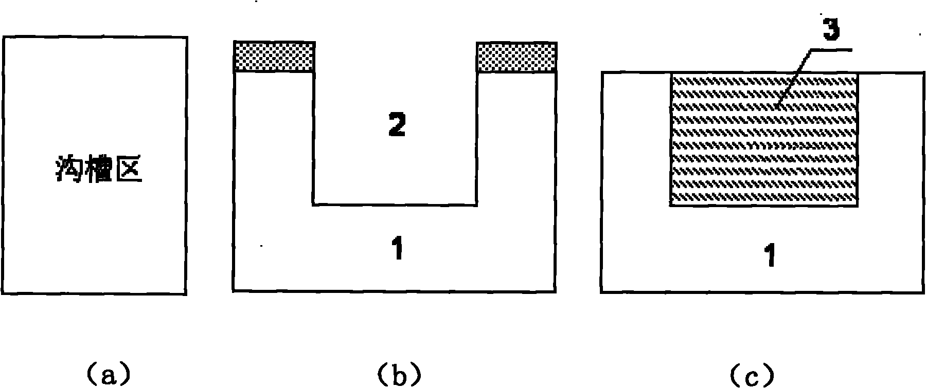
[0047] In the following embodiment, a wide and deep trench with a length of 10 μm, a width of 10 μm, and a depth of 5 μm is used as an example to illustrate the method of the present invention, and the accompanying drawings are only for better understanding of the method of the present invention Implementation process, not drawn to scale. In addition, the wide and deep grooves mentioned in the present invention refer to wide and deep grooves with a width greater than 2.0 μm and a depth greater than 2.0 μm.

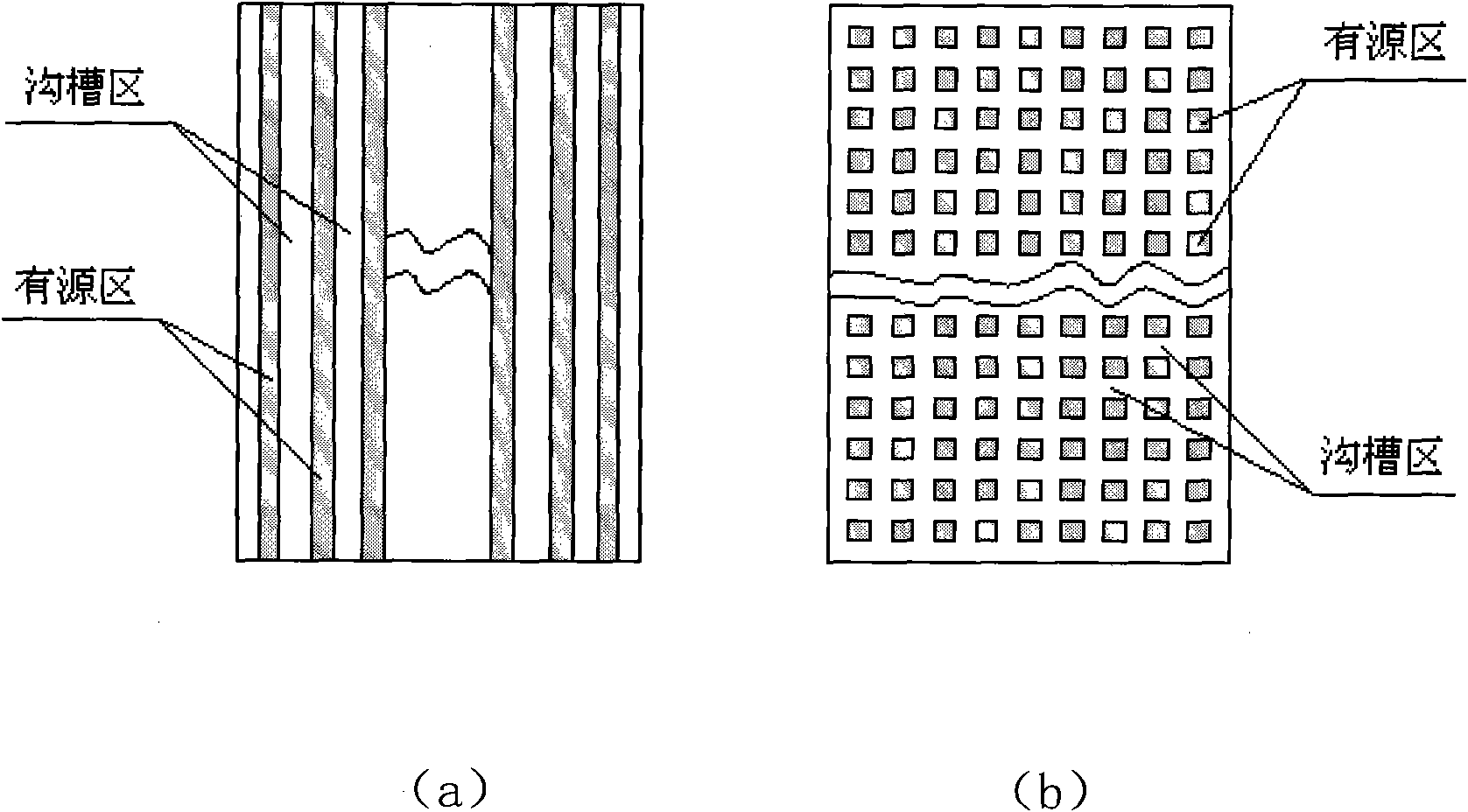
[0048] see figure 2 As shown, the wide and deep trench described in the present invention is not directly forming a wide and deep trench with a length of 10 μm, a width of 10 μm, and a depth of 5 μm on the silicon wafer, but is improved during the layout design. Within the range of 10 μm, a plurality of elongated small grooves with equal intervals, or a plurality of small silicon units are formed. For example, using elongated small grooves, the length of each elongated ...


PUM


Abstract

The invention discloses a method for manufacturing wide and deep trenches by medium filling, which comprises the following steps of: sequentially growing a layer of bottom-layer oxide film, a silicon nitride film and a top-layer oxide film on a silicon wafer; coating a photoresist on the top-layer oxide film, and defining a plurality of trenches at an equal interval by photoetching; removing the exposed top-layer oxide film by etching, and then removing the photoresist; etching the silicon nitride film, the bottom-layer oxide film and the silicon wafer by utilizing a pattern of the top-layer oxide film as a mask to obtain the plurality of required trenches; oxidizing all the sidewalls of the plurality of trenches by thermal oxidation to form silicon oxide sidewalls; removing the top-layer oxide film and the silicon nitride film; depositing a required medium film by chemical vapor deposition, and filling the trenches; and removing the medium film on the surface of the silicon wafer by back-etching or chemical mechanical grinding, and removing the oxide film on the surface of the silicon wafer to obtain the wide and deep trenches filled with the medium film. In the method, the filling of the wide and deep trenches is realized by utilizing a proven process in combination with the innovation of the pattern.

Description

technical field [0001] The invention relates to a manufacturing process method of a semiconductor integrated circuit, in particular to a manufacturing method for wide and deep trench dielectric filling. Background technique [0002] Wide and deep trenches (such as 10 μm wide and 5 μm deep) have important applications in low-capacitance transient diodes and REDUCED SURFACE FIELD-RESURF technologies for high-voltage devices. In low-capacitance transient diodes, in order to obtain low capacitance to improve device performance, it is necessary to use wide and deep dielectric-filled trenches; in high-voltage device processes, wide and deep dielectric-filled trenches can be used to reduce The surface electric field increases the breakdown voltage of the device. [0003] Trench depths in shallow trench processes are typically less than 5000 Angstroms. For such a relatively shallow trench, even if the trench width is greater than 10 μm, the trench can be filled by depositing a fil...

Claims


Application Information

Patent Timeline
IPC IPC(8): H01L21/762
Inventor 肖胜安
Owner SHANGHAI HUAHONG GRACE SEMICON MFG CORP
Why Eureka
Try Eureka