

Method for preparing magnetic sensitive microstructure unit by femtosecond laser non-mask method
A femtosecond laser and magnetically sensitive technology, which is applied in the manufacture of microstructure devices, microstructure technology, microstructure devices, etc., can solve the problem of long production cycle, difficult micro-nanoscale processing, unsuitable for single-piece, small-batch production and Problems such as the trial production of new products, to achieve the effect of short pulse duration
- Summary
- Abstract
- Description
- Claims
- Application Information
AI Technical Summary
Problems solved by technology
Method used
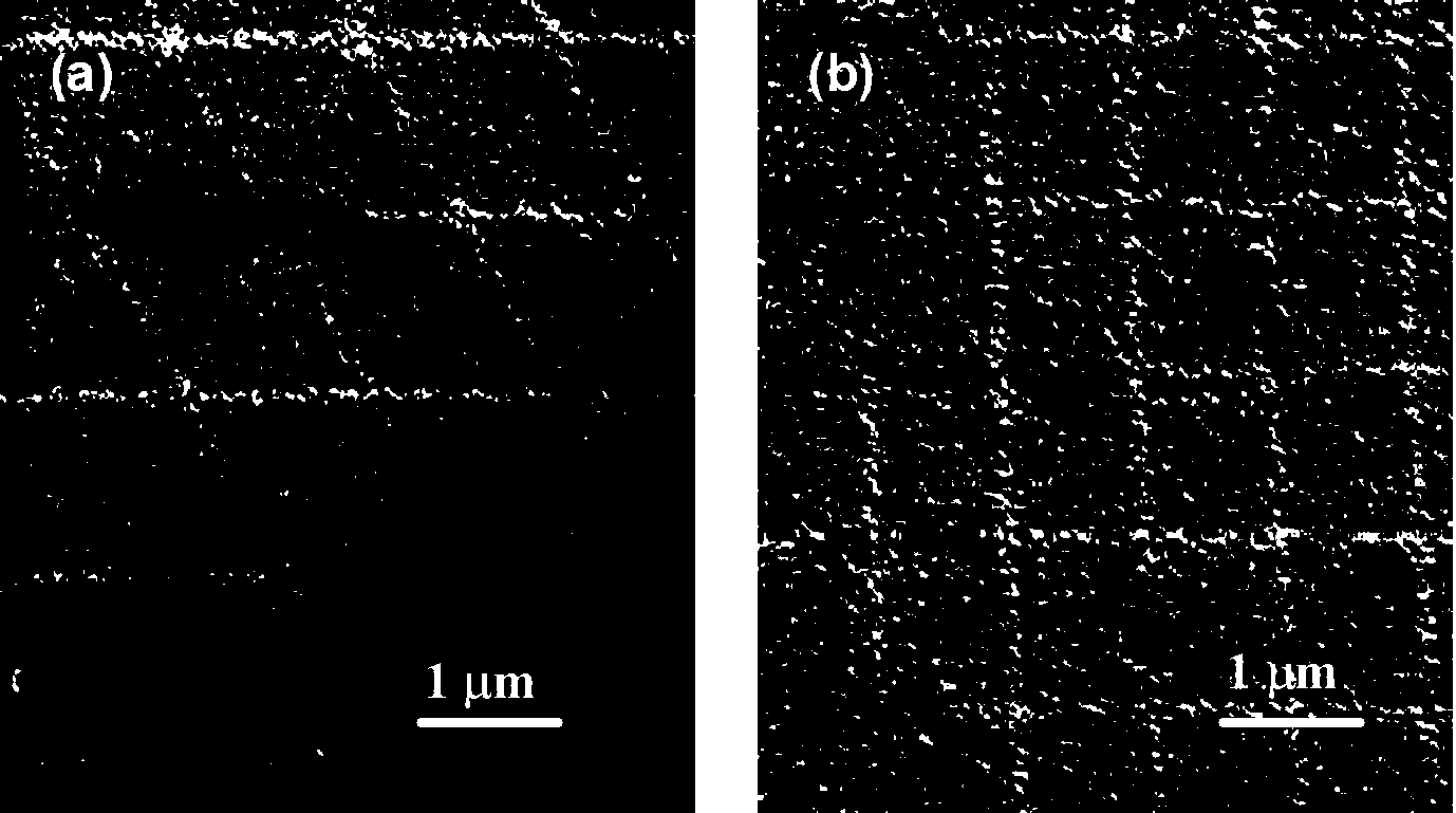
Image

Examples
Embodiment 1
[0014] Embodiment 1: Prepare the magnetically sensitive microstructure unit according to the following steps
[0015] Step 1: Deposit a buffer layer Cr with a thickness of 5nm and a ferromagnetic layer CoPt with a thickness of 40nm on the cleaned single crystal silicon substrate by using high-vacuum magnetron sputtering equipment to obtain a magnetic recording film; wherein, the growth conditions of the magnetic layer For: back vacuum 5×10 -6 Pa; sputtering pressure 0.3Pa; sputtering power 10W; argon flow rate 20sccm; substrate temperature 100°C;
[0016] Step 2. Use femtosecond laser as light source to irradiate the magnetic thin film. After the irradiation is completed, a triangular magnetically sensitive microstructure unit is obtained; wherein, the parameters of the femtosecond laser are: single pulse energy 5 μJ; pulse width 90fs ; Wavelength 800nm; Pulse frequency 50Hz; Among them, an induced magnetic field of 500Oe is applied along the direction perpendicular to the su...
Embodiment 2
[0017] Example 2: Prepare the magnetically sensitive microstructure unit according to the following steps
[0018] Step 1, using high vacuum magnetron sputtering equipment to deposit a magnetic layer Tb-Dy-Fe with a thickness of 500nm and a protective layer Ta with a thickness of 5nm on the cleaned glass substrate to obtain a giant magnetostrictive film; The growth condition of the layer is: background vacuum 5×10 -6 Pa; sputtering pressure 0.5Pa; sputtering power 120W; argon flow 20sccm; substrate temperature 300°C;
[0019] Step 2. Use femtosecond laser as light source without applying an induced magnetic field to irradiate the magnetic thin film. After the irradiation is completed, a magnetically sensitive microstructure unit with a unit shape of a rectangle is obtained; wherein, the parameters of the femtosecond laser are: single pulse energy 50 μJ The pulse width is 100fs; the wavelength is 800nm; the pulse frequency is 100Hz; the moving track of the sample stage is pr...
Embodiment 3
[0020] Example 3: Prepare the magnetically sensitive microstructure unit according to the following steps
[0021] Step 1, utilize high-vacuum magnetron sputtering equipment to deposit a buffer layer Ta with a thickness of 5nm, a CoFe ferromagnetic layer with a thickness of 5nm, an IrMn antiferromagnetic layer with a thickness of 12nm, and a thickness of 12nm on the cleaned single crystal silicon substrate. A protective layer Ta of 8nm was obtained to obtain a ferromagnetic / antiferromagnetic double-layer film; wherein, the growth condition of the magnetic layer was: background vacuum 5×10 -6 Pa; sputtering pressure 0.3Pa; sputtering power 30W; argon flow 20sccm; substrate temperature at room temperature;
[0022] Step 2. Use femtosecond laser as light source to irradiate the magnetic thin film. After the irradiation is completed, a magnetically sensitive microstructure unit whose unit shape is a regular hexagon is obtained; wherein, the parameters of the femtosecond laser ar...
PUM
| Property | Measurement | Unit |
|---|---|---|
| size | aaaaa | aaaaa |
| thickness | aaaaa | aaaaa |
| thickness | aaaaa | aaaaa |
Abstract
Description
Claims
Application Information