Femtosecond laser etching method to enhance the performance of amorphous silicon thin film solar cells

A technology of solar cells and amorphous silicon thin films, applied in photovoltaic power generation, circuits, electrical components, etc., can solve the problems of inadaptability to amorphous silicon thin film solar cells, etc., achieve shortened interaction time, simple operation process, smooth surface and smooth effect

Inactive Publication Date: 2018-07-10
BOHAI UNIV
View PDF5 Cites 0 Cited by
  • Summary
  • Abstract
  • Description
  • Claims
  • Application Information

AI Technical Summary

Problems solved by technology

However, the method for preparing the textured surface of the anti-reflection layer is not suitable for amorphous silicon thin film solar cells with an absorbing layer thickness of only 1-2 μm.

Method used


Image

  • Femtosecond laser etching method to enhance the performance of amorphous silicon thin film solar cells
  • Femtosecond laser etching method to enhance the performance of amorphous silicon thin film solar cells
  • Femtosecond laser etching method to enhance the performance of amorphous silicon thin film solar cells

Examples


Embodiment

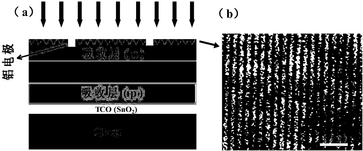
[0042] Such as figure 2 As shown, the femtosecond laser pulse texture etching period T is a certain value, and the femtosecond laser pulse energy W is changed to prepare the porous microstructure anti-reflection layer on the surface of the amorphous silicon thin film solar cell as follows:

[0043] 1.1. Adhere the amorphous silicon thin-film solar cell to the glass slide, and then fix it on the femtosecond laser micro-nano processing platform. 2 ;

[0044] 1.2. The femtosecond laser pulse is focused on the surface of the n-type amorphous silicon film of the thin-film solar cell through a microscope system with a 10× objective lens (numerical aperture of 0.25), forming a spot with a beam waist radius of about 0.5 μm;

[0045] 1.3. Controlled by the computer terminal, the focused femtosecond laser pulse will move at a constant speed along the vertical direction of the platform at a rate of 1mm / s, set the repetition frequency of the femtosecond laser pulse to 1kHz, and set the ...

Embodiment 1

[0074] 1.1. Adhere the amorphous silicon thin-film solar cell prepared in Comparative Example 1 to a glass slide, and then fix it on the femtosecond laser micro-nano processing platform. The stepping accuracy of the platform motor is 0.1 μm, and the solar cell size is 1.5×1.5cm 2 ;

[0075] 1.2. The femtosecond laser pulse is focused on the surface of the n-type amorphous silicon film of the thin-film solar cell through a microscope system with a 10× objective lens (numerical aperture of 0.25), forming a spot with a beam waist radius of about 0.5 μm;

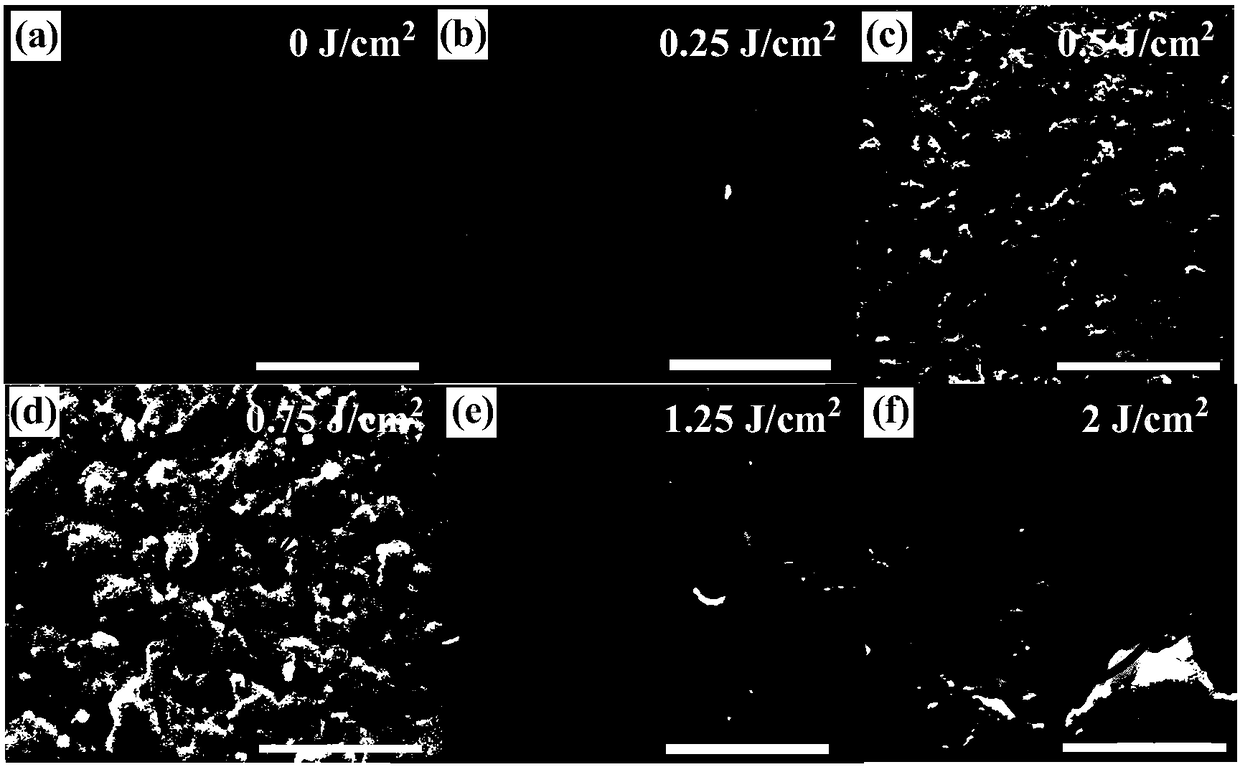
[0076] 1.3. Controlled by the computer terminal, the focused femtosecond laser pulse will move at a constant speed along the vertical direction of the platform at a rate of 1mm / s. Pulse etching period T is 15μm, laser pulse energy (W) 0.5J / cm 2 According to the micromachining parameters, the linearly polarized femtosecond laser pulse will texture the surface of the n-type amorphous silicon film of the amorphous silicon thin fil...

Embodiment 2

[0078] 1.1. Adhere the amorphous silicon thin-film solar cell prepared in Comparative Example 1 to a glass slide, and then fix it on the femtosecond laser micro-nano processing platform. The stepping accuracy of the platform motor is 0.1 μm, and the solar cell size is 1.5×1.5cm 2 ;

[0079] 1.2. The femtosecond laser pulse is focused on the surface of the n-type amorphous silicon film of the thin-film solar cell through a microscope system with a 10× objective lens (numerical aperture of 0.25), forming a spot with a beam waist radius of about 0.5 μm;

[0080] 1.3. Controlled by the computer terminal, the focused femtosecond laser pulse will move at a constant speed along the vertical direction of the platform at a rate of 1mm / s. Pulse etching period T is 15μm, laser pulse energy (W) 0.75J / cm 2 According to the micromachining parameters, the linearly polarized femtosecond laser pulse will texture the surface of the n-type amorphous silicon film of the amorphous silicon thin fi...


PUM


Abstract

A method for enhancing the performance of amorphous silicon thin-film solar cells by femtosecond laser etching. The p-i-n structured amorphous silicon thin-film solar cells are fixed on a femtosecond laser micro-nano processing platform, and femtosecond laser pulses pass through a 10-fold objective lens The microscope system is vertically incident and focused on the surface of the n-type amorphous silicon film of the thin-film solar cell; the linearly polarized femtosecond laser pulse will velvet the surface of the n-type amorphous silicon film of the amorphous silicon thin-film solar cell to obtain an efficient p‑i‑n structure amorphous silicon thin film solar cells. The method has the advantages of simple process, low cost, remarkable improvement in photoelectric conversion performance, and the photoelectric conversion efficiency of the obtained solar cell reaches 14.9%, which is twice the conversion efficiency of the untreated amorphous silicon thin film solar cell.

Description

technical field [0001] The invention relates to the technical field of nanomaterial preparation, in particular to a method for preparing an anti-reflection layer on the surface of a solar cell by a femtosecond laser pulse etching method to enhance the performance of an amorphous silicon thin film solar (a-SiTFSCs) cell. Background technique [0002] At present, environmental pollution and shortage of traditional energy sources (including oil, coal and natural gas) have become two major problems restricting the economic development of countries all over the world. As a device that can directly convert solar radiation light energy into electrical energy, solar cells do not need to consume traditional energy during the photoelectric conversion process, and at the same time, there is no environmental pollution at all. It is a very promising optoelectronic semiconductor. conversion device. At present, the types of solar cells being researched by various countries mainly include ...

Claims


Application Information

Patent Timeline
Patent Type & Authority Patents(China)
IPC IPC(8): H01L31/18
CPCH01L31/1804Y02E10/547Y02P70/50
Inventor 邵珠峰杨秀娟朱革张宇峰曲士良
Owner BOHAI UNIV
Why Eureka
Try Eureka