Preparation method of deep sub-wavelength periodic stripe structure on surface of wide bandgap semiconductor

A wide-bandgap semiconductor, deep subwavelength technology, used in welding equipment, manufacturing tools, laser welding equipment, etc., can solve the problem of femtosecond laser absorption-limited multiphoton ionization and tunnel ionization, and periodic fringe structure and morphology. control, wide-bandgap semiconductor processing and application difficulties, etc., to achieve the effect of easy control, high concentration doping, and lower ablation threshold

Inactive Publication Date: 2020-12-18
NANKAI UNIV
View PDF8 Cites 1 Cited by
  • Summary
  • Abstract
  • Description
  • Claims
  • Application Information

AI Technical Summary

Problems solved by technology

However, due to the wide bandgap of wide-bandgap semiconductors and their transparency to visible and near-infrared light, their absorption of femtosecond lasers is limited by multi-photon ionization and tunnel ionization, and the ablation threshold is usually higher than that of metals and semiconductors.
Under high-energy flow, the ablation of the material surface is severe, and the laser-induced periodic stripe structure morphology is difficult to control
In addition, the laser-induced stripe period greatly depends on the laser fluence and decreases as the fluence decreases. If the ablation threshold fluence cannot be further reduced, it will be difficult to form a finer deep subwavelength stripe structure
[0004] This laser processing problem caused by the nature of the material itself has brought great difficulties to the processing and application of wide bandgap semiconductors.

Method used


Image

  • Preparation method of deep sub-wavelength periodic stripe structure on surface of wide bandgap semiconductor
  • Preparation method of deep sub-wavelength periodic stripe structure on surface of wide bandgap semiconductor

Examples


Embodiment Construction

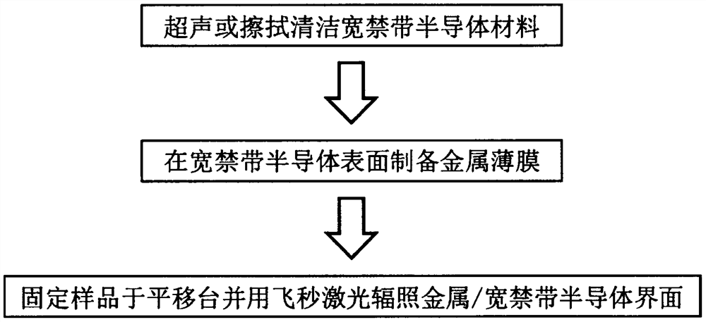
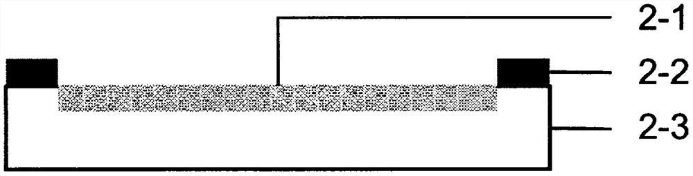
[0024] The following will clearly and completely describe the technical solutions in the embodiments of the present invention with reference to the accompanying drawings in the embodiments of the present invention. Obviously, the described embodiments are only part of the embodiments of the present invention, not all of them. Based on the embodiments of the present invention, all other embodiments obtained by persons of ordinary skill in the art without making creative efforts belong to the protection scope of the present invention. Additionally, the protection scope of the present invention should not be limited only to the following specific structures or components or specific parameters.

[0025] In order to describe the technical means and efficacy of the present invention in more detail, the preparation of the deep sub-wavelength periodic stripe structure on the surface of wide-bandgap semiconductor proposed by the present invention will be described in detail below in co...


PUM


Abstract

The invention discloses a preparation method of deep sub-wavelength periodic stripes on the surface of a wide bandgap semiconductor. Femtosecond laser processing is assisted in forming the deep sub-wavelength periodic stripe structure in an irradiation area in a manner of pre-plating a metal film on the surface of a wide bandgap semiconductor material. By utilization of the metal/wide bandgap semiconductor composite structure, in the femtosecond laser irradiation process, absorption of the material to incident light energy can be greatly enhanced, and the interaction efficiency of femtosecondlaser and the wide bandgap material is improved. According to the method, the effect of reducing an ablation threshold of the material is obvious, and the formed deep sub-wavelength stripe period is fine. The method also has the advantages of simple process, wide applicability, strong flexibility and the like. Deep sub-wavelength stripes with different shapes and different space periods on the wide bandgap semiconductor can be realized by designing femtosecond laser energy flow, pulse number and processing area patterns.

Description

technical field [0001] The invention relates to the field of material processing, in particular to a method for preparing a deep sub-wavelength periodic stripe structure on the surface of a wide-bandgap semiconductor by laser processing, and belongs to the technical field of femtosecond laser micro-nano processing. Background technique [0002] Wide bandgap semiconductors represented by silicon carbide (3.26eV), gallium nitride (3.4eV), zinc oxide (3.37eV), etc. are called third-generation semiconductors. Compared with the first-generation (Si / Ge) and second-generation semiconductors (gallium arsenide (GaAs), indium antimonide (InSb)) materials, the third-generation semiconductors have a wide band gap and a high breakdown electric field. High thermal conductivity, high electron saturation rate and higher radiation resistance, suitable for high temperature, high frequency, radiation resistance and high power devices. In addition, due to the high luminous efficiency and high ...

Claims


Application Information

Patent Timeline
Patent Type & Authority Applications(China)
IPC IPC(8): B23K26/0622B23K26/082B23K26/122B23K26/14B23K26/70
CPCB23K26/14B23K26/0624B23K26/082B23K26/1224B23K26/702
Inventor 吴强刘瑶瑶王俞萱黄松李志轩进晓荣符显辉周旭宋冠廷胡晓洋江欣达姚江宏许京军
Owner NANKAI UNIV
Why Eureka
Try Eureka