Printed circuit board (PCB) signal group delay analysis system and method

A printed circuit board and delay analysis technology, which is applied in the direction of electronic circuit testing, electrical digital data processing, special data processing applications, etc., can solve problems such as impossibility, frequency problems, system operation failure, etc., and achieve the effect of correct timing relationship

Inactive Publication Date: 2013-01-02
HONG FU JIN PRECISION IND (SHENZHEN) CO LTD +1
View PDF7 Cites 9 Cited by
  • Summary
  • Abstract
  • Description
  • Claims
  • Application Information

AI Technical Summary

Problems solved by technology

However, in the real circuit layout, the signal time delay is affected by many factors, such as perforation, crosstalk effect, PCB material, stacked board structure, etc., which is not suitable for the rough estimation relationship of the commonly used time delay of about 6mil per second. make an estimate
[0003] Generally speaking, in order to keep the frequency signal working normally, it is necessary to regulate the length of the DATA signal line and the CLOCK signal line to be equal in length when winding the PCB board, but it is impossible to do so in practice.
Therefore, the general design often stipulates that the relative length of the DATA signal line and the CLOCK signal line must be within a certain range, otherwise it is easy to cause frequency problems and cause the system to fail.

Method used


Image

  • Printed circuit board (PCB) signal group delay analysis system and method
  • Printed circuit board (PCB) signal group delay analysis system and method
  • Printed circuit board (PCB) signal group delay analysis system and method

Examples


Embodiment Construction

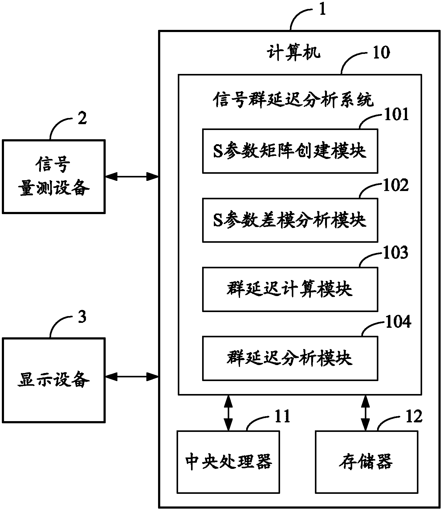
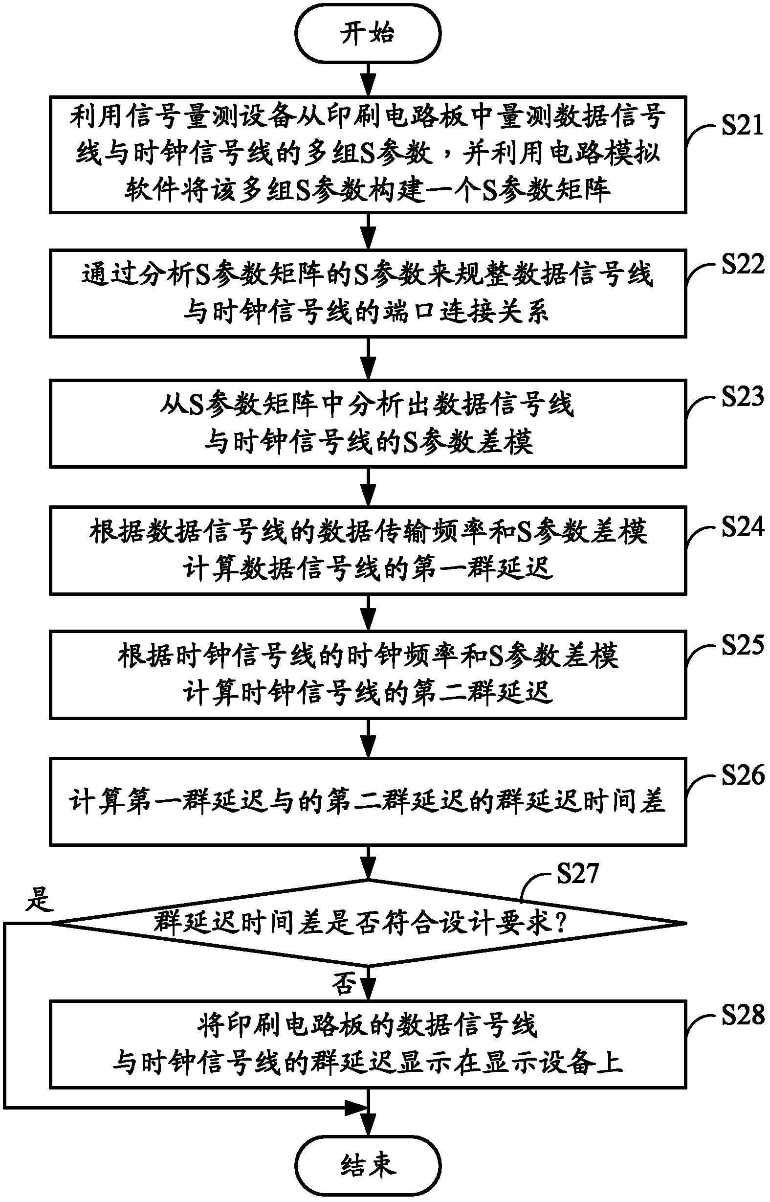
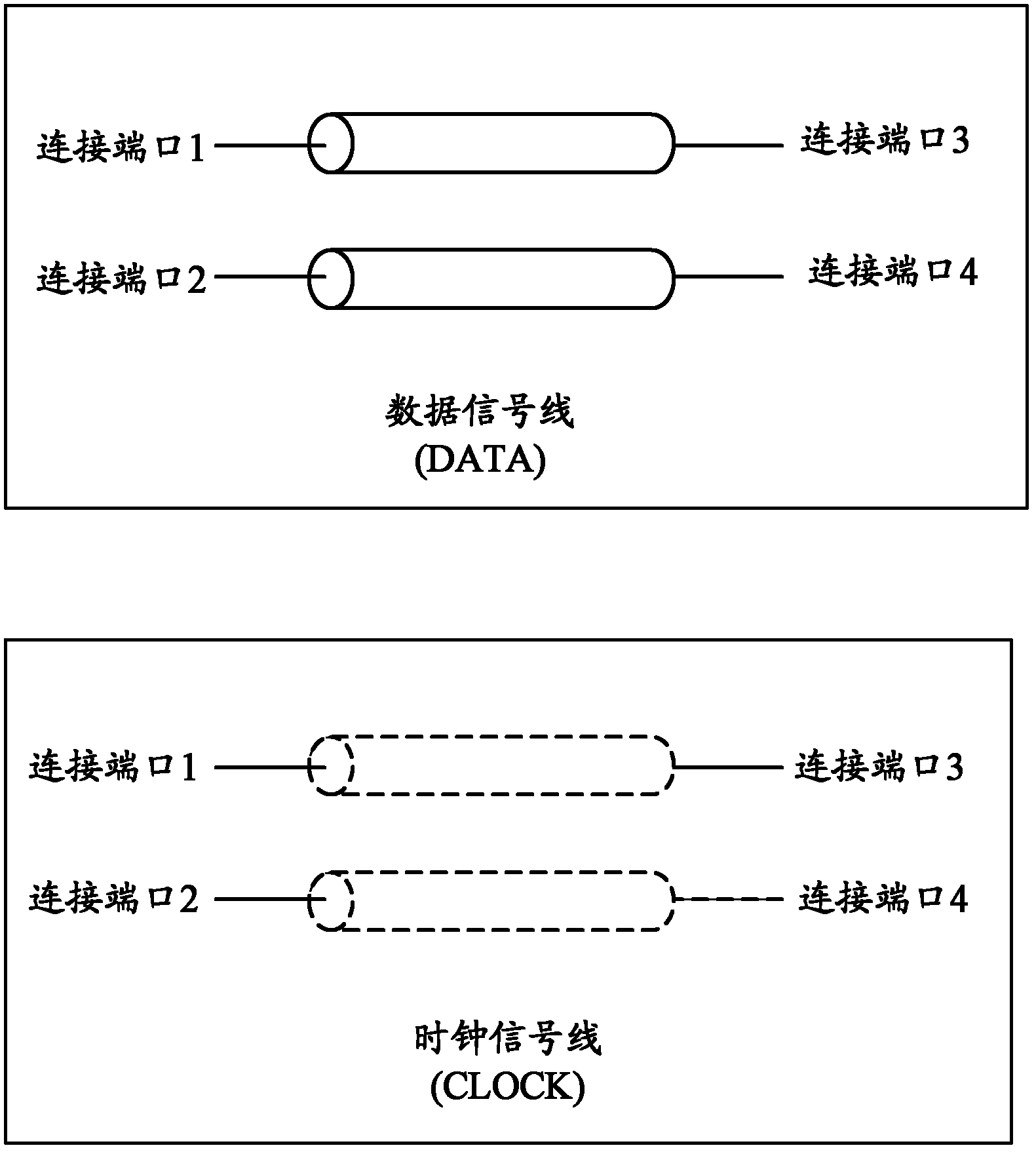
[0023] Such as figure 1 Shown is a structure diagram of a preferred embodiment of the system 10 for analyzing the signal group delay of the printed circuit board of the present invention. The printed circuit board (Printed Circuit Board, PCB) includes, but is not limited to, the circuit boards of computer motherboards, game machines, and household appliances. The signal group delay (Signal Group Delay) is defined as the delay time of each signal corresponding to each frequency, which is represented by the slope change of the signal transmission channel phase versus frequency. In this embodiment, the signal transmission channel includes a data (DATA) signal line and a frequency (CLOCK) signal line, refer to image 3 As shown, when wiring a printed circuit board, there may be multiple sets of data signal lines, but generally there is only one set of clock signal lines. The data signal line is used for data transmission between electronic components in the printed circuit board...


PUM


Abstract

The invention discloses a printed circuit board (PCB) signal group delay analysis system and a PCB signal group delay analysis method. The method comprises the following steps of: measuring S parameters of a data signal line and a clock signal line from the PCB; normalizing a connecting port between the data signal line and the clock signal line by analyzing the S parameters; analyzing an S parameter differential mode of the data signal line and the clock signal line; calculating the first group delay of the data signal line according to the data transmission frequency and S parameter differential mode of the data signal line; calculating the second group delay of the clock signal line according to the clock frequency and S parameter differential mode of the clock signal line; calculating the group delay time difference of the first group delay and the second group delay; and displaying the group delay between the data signal line and the clock signal line on display equipment when the group delay time difference does not meet the design requirements. According to the method, whether the relative length of the data signal line and the clock signal line is equivalent can be estimated, so that an accurate timing sequence relationship of wiring signals in the PCB is kept.

Description

technical field [0001] The invention relates to a signal time delay evaluation system and method, in particular to a signal group delay analysis system and method of a printed circuit board. Background technique [0002] When evaluating the signal time delay of circuit layout, the most concerned feature is whether the relative lengths of the data (DATA) signal line and the frequency (CLOCK) signal line are equivalent, so as to keep the timing relationship of the signal correct. However, in the real circuit layout, the signal time delay is affected by quite a few factors, such as perforation, crosstalk effect, PCB material, stacked board structure, etc., which is not suitable for the rough estimation relationship of the commonly used time delay of about 6mil per second. Make an estimate. [0003] Generally speaking, in order to keep the frequency signal working normally, it is necessary to regulate the length of the DATA signal line and the CLOCK signal line to be equal in l...

Claims


Application Information

Patent Timeline
IPC IPC(8): G01R31/28G06F17/50
Inventor 谢博全陈俊仁赖盈佐张恩硕
Owner HONG FU JIN PRECISION IND (SHENZHEN) CO LTD
Why Eureka
Try Eureka