Touch device and touch display device

A touch device, touch panel technology, applied in the direction of instruments, electrical digital data processing, data processing input/output process, etc., can solve anti-reflective film creases, increased labor costs, and the overall thickness of the touch device can not be effective Reduced ground and other issues to achieve the effect of reducing light reflectivity

Inactive Publication Date: 2013-01-02
WINTEK CHINA TECH LTD +1
View PDF4 Cites 6 Cited by
  • Summary
  • Abstract
  • Description
  • Claims
  • Application Information

AI Technical Summary

Problems solved by technology

As a result, the overall thickness of the touch device 100 in the prior art cannot be effectively reduced, thereby reducing the competitive advantage of the touch device product
[0003] In addition, when figure 1 In the case where the optical adhesive 120, the electromagnetic shielding film 130, and the anti-reflection film 140 in the touch device 100 shown are plastic substrates with optical adhesives, in production, when the electromagnetic shielding film 130 and the anti-reflection film 140 are pasted When it is used, it is easy to cause defects such as bubbles and foreign objects, increase labor costs, and the anti-reflective film is likely to cause creases on the anti-reflective film due to the manual operation method.

Method used


Image

  • Touch device and touch display device
  • Touch device and touch display device
  • Touch device and touch display device

Examples


Embodiment Construction

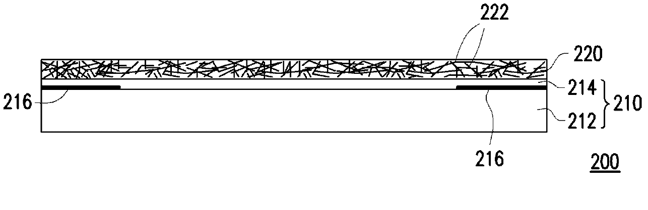
[0026] figure 2 It is a partial cross-sectional schematic diagram of the touch device of the present invention. Please refer to figure 2 , the touch device 200 includes a touch panel 210 and a shielding electrode film 220 . The touch panel 210 includes a substrate 212 and a touch element 214, wherein the touch element 214 is located on the substrate 212, and the substrate 212 is a glass plate or a plastic plate. In this embodiment, the substrate 212 is provided with a decorative layer 216 to The substrate 212 and the decoration layer 216 form a cover lens, such as figure 2 As shown, the decorative layer 216 is located between the substrate 212 and the touch element 214, and the decorative layer 216 is composed of at least one of diamond-like, ceramic, ink and photoresist materials, but the present invention does not limit the arrangement of the decorative layer location and material.

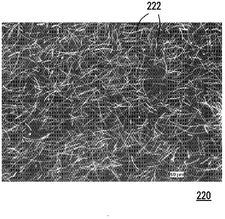
[0027] Please continue to refer to figure 2 The shielding electrode film 220 is dis...


PUM


Abstract

A touch device comprises a touch panel and a shielding electrode film. The touch panel comprises a substrate and a touch element located on the substrate. The shielding electrode film is configured on the touch panel and is provided with a plurality of nanometer metal wires which are staggered to form the shielding electrode film. Therefore, the touch device can greatly reduce integral thickness. A touch display device with the structure is further provided.

Description

technical field [0001] The present invention relates to a touch device and a touch display device, and in particular to a thinned touch device and a touch display device. Background technique [0002] figure 1 It is a sectional view of a touch device in the prior art. Please refer to figure 1 In order to improve the operating characteristics of the elements of the touch panel 110 in the prior art touch device 100, an electromagnetic shielding film 130 is usually attached to the surface of the touch panel 110 with optical glue 120, thereby increasing the signal-to-noise ratio of the touch panel , wherein the electromagnetic shielding film 130 is an indium tin oxide film. In addition, in order to improve the overall light transmittance and reduce the light reflectance of the touch device, an anti-reflection film 140 must be added on the touch panel 110 in the prior art. And a transparent cover plate 150 is disposed on the other surface of the touch panel 110 . As a result...

Claims


Application Information

Patent Timeline
Patent Type & Authority Applications(China)
IPC IPC(8): G06F3/041
Inventor 林怡君吴明坤黄炳文
Owner WINTEK CHINA TECH LTD
Why Eureka
Try Eureka