

Laminated high melting point soldering layer and fabrication method for the same, and semiconductor device
A high-melting-point metal layer and high-melting point technology, which is applied in semiconductor devices, semiconductor/solid-state device manufacturing, semiconductor/solid-state device components, etc., can solve problems such as complex conductive metal components, shorten process time, increase large-scale The effect of throughput efficiency
- Summary
- Abstract
- Description
- Claims
- Application Information
AI Technical Summary
Problems solved by technology
Method used
Image

Examples
Embodiment
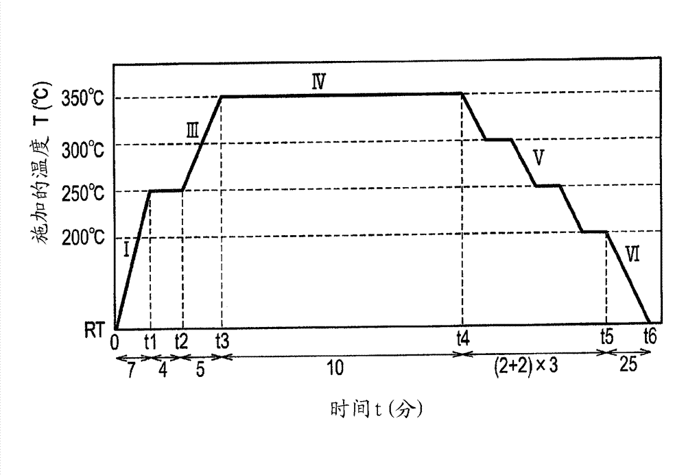
[0051] (Arrangement of laminated high melting point solder layers)
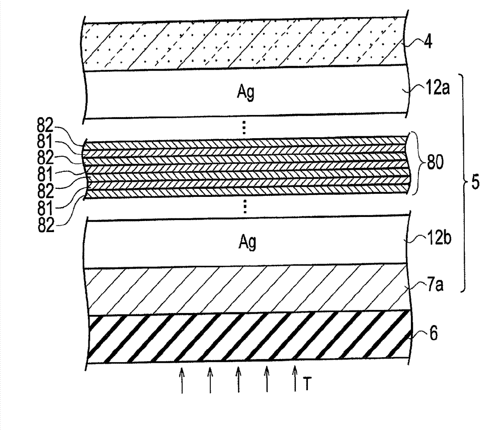
[0052] 1A is a schematic cross-sectional configuration diagram showing a laminated high melting point solder layer 5 according to an embodiment, and FIG. 1B is a schematic cross-sectional configuration diagram of a laminated structure 80 that laminates a plurality of three layers Each three-layer structure includes a low melting point metal thin film layer 81, and a high melting point metal thin film layer 82 placed on the surface and back surface of the low melting point metal thin film layer 81.
[0053] As shown in FIGS. 1A and 1B , the laminated high-melting-point soldering layer 5 according to the embodiment includes: a laminated structure 80 stacking a plurality of three-layer structures, each of which includes a low-melting-point metal thin film layer 81 , and placed The surface of the low-melting-point metal film layer 81 and the high-melting-point metal film layer 82 on the back surface; the first hi...
PUM
| Property | Measurement | Unit |
|---|---|---|
| Band gap energy | aaaaa | aaaaa |
Abstract
Description
Claims
Application Information