Thin film transistor array substrate and display device

A technology of thin film transistors and array substrates, applied in the display field, can solve the problems of many wirings and complexity, and achieve the effects of reducing wiring quantity, complexity and cost.

Active Publication Date: 2013-01-02
BEIJING BOE OPTOELECTRONCIS TECH CO LTD
View PDF6 Cites 14 Cited by
  • Summary
  • Abstract
  • Description
  • Claims
  • Application Information

AI Technical Summary

Problems solved by technology

[0004] In the existing driving method, each row of pixel units needs to correspond to a scanning line, and each column of sub-pixel units corresponds to a data line, and the wiring is more complicated.

Method used


Image

  • Thin film transistor array substrate and display device
  • Thin film transistor array substrate and display device
  • Thin film transistor array substrate and display device

Examples


Embodiment Construction

[0017] In order to reduce the amount of wiring on the array substrate, reduce complexity and save cost, an embodiment of the present invention provides a thin film transistor (TFT) array substrate.

[0018] Preferred embodiments of the present invention will be described in detail below in conjunction with the accompanying drawings.

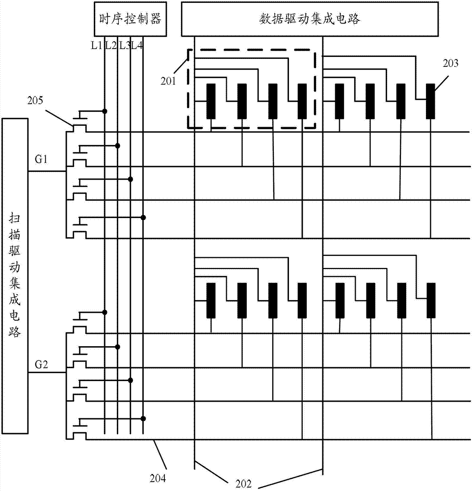
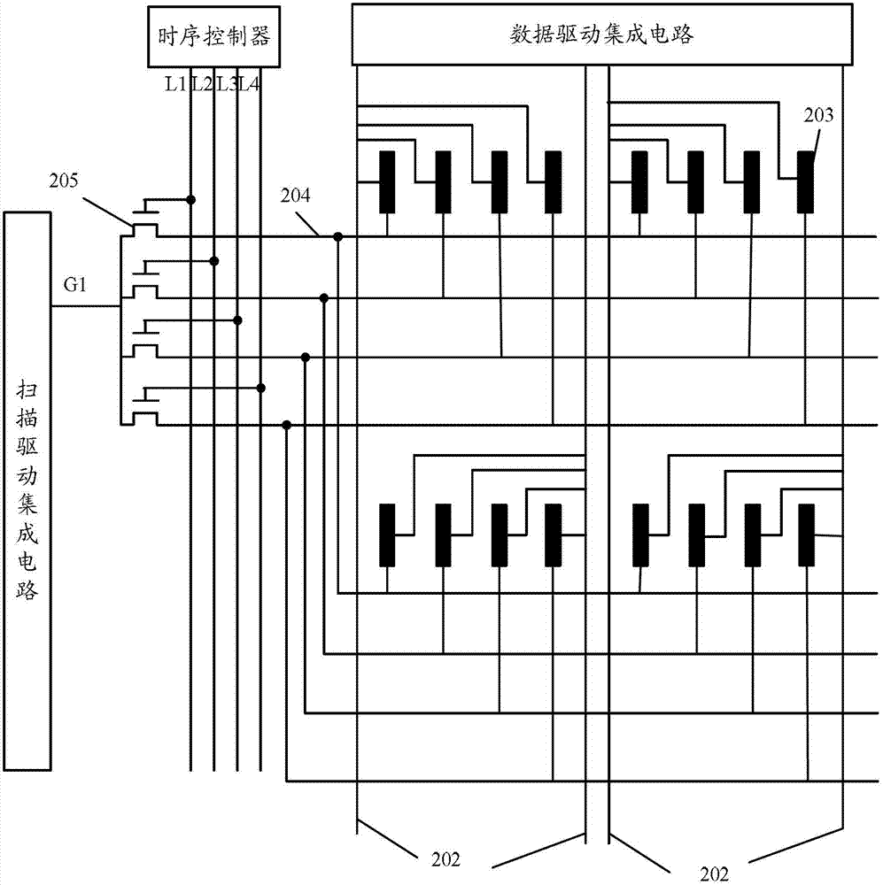
[0019] In the following embodiments, the horizontal distribution of scanning driving lines (that is, gate driving lines) and the vertical distribution of data lines are taken as examples for illustration. In practical applications, the vertical distribution of scanning driving lines and the horizontal distribution of data lines may also be used. Figure 2a with 2b Rotate to the left or right by 90° to obtain the vertical distribution of the scanning driving lines and the horizontal distribution of the data lines. For these two cases, the connection between the scanning driving lines and each pixel unit and the connection relationship between the ...


PUM


Abstract

The invention discloses a thin film transistor array substrate and a display device, and aims to reduce the wiring amount of the array substrate, reduce the complexity and save the cost. The array substrate comprises a pixel unit array, wherein any column of pixel units correspond to one or two data wires; in the same column of pixel units, sub pixels belonging to the same pixel unit are connected to the same data wire; for any row of pixel units, grid lines are arranged, and the number of grid lines is the same as that of sub pixels involved in each pixel unit; the sub pixels belonging to the same pixel unit are respectively connected to different grid lines; the grid lines are respectively connected with electronic switches and then are connected to the same grid driving signal; the control ends of the electronic switches are respectively connected with time sequence control signals; and the time sequence control signals control the electronic switches to be turned on or turned off at different moments.

Description

technical field [0001] The present invention relates to the field of display technology, in particular to a thin film transistor (Thin Film Transistor, TFT) array substrate and a display device. Background technique [0002] In the existing thin-film transistor-liquid crystal display (TFT-LCD), the liquid crystal display panel is formed by filling liquid crystal between the thin-film transistor array substrate and the color filter substrate after boxing the thin-film transistor array substrate and the color filter substrate. [0003] Among them, the thin film transistor array substrate includes a plurality of pixel units. In the current mainstream thin film transistor array substrate in the market, each pixel unit consists of three sub-pixels for red (R), green (G) and blue (B) color display respectively. Composition of pixel units. as attached figure 1 As shown, it is a schematic structural diagram of an existing TFT-LCD array substrate, including a base substrate 101, an...

Claims


Application Information

Patent Timeline
IPC IPC(8): H01L27/02G09G3/20G02F1/1362
Inventor 刘磊
Owner BEIJING BOE OPTOELECTRONCIS TECH CO LTD
Why Eureka
Try Eureka