Light-emitting element mounting substrate and LED package

A technology for light-emitting components and substrates, applied in electrical components, semiconductor devices, electric solid-state devices, etc., can solve the problems of difficulty in obtaining heat dissipation, loss of competitiveness, and high prices, and achieve the effect of excellent heat dissipation and light reflectivity.

Inactive Publication Date: 2013-01-02
SHINDOU DENSHI INDS
View PDF5 Cites 8 Cited by
  • Summary
  • Abstract
  • Description
  • Claims
  • Application Information

AI Technical Summary

Problems solved by technology

[0008] However, as a form of a double-sided wiring board, if it has through holes for ensuring heat dissipation and fineness of wiring, it will inevitably be more expensive than a single-sided wiring board, so it becomes the price per unit brightness ( JPY / lm) index loses competitiveness
In addition, in a structure in which heat is dissipated through a through-hole whose cross-sectional area is smaller than the size of the LED chip, it is difficult to obtain sufficient heat dissipation.
[0009] In addition, if a flip-chip LED chip is to be mounted on a wiring substrate other than a ceramic substrate, the directly below the LED chip and the vicinity of the LED chip are not white like the ceramic substrate. The reason why the light beam of the LED chip is reduced

Method used


Image

  • Light-emitting element mounting substrate and LED package
  • Light-emitting element mounting substrate and LED package
  • Light-emitting element mounting substrate and LED package

Examples


no. 1 approach

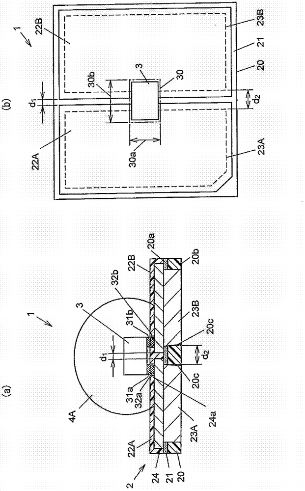
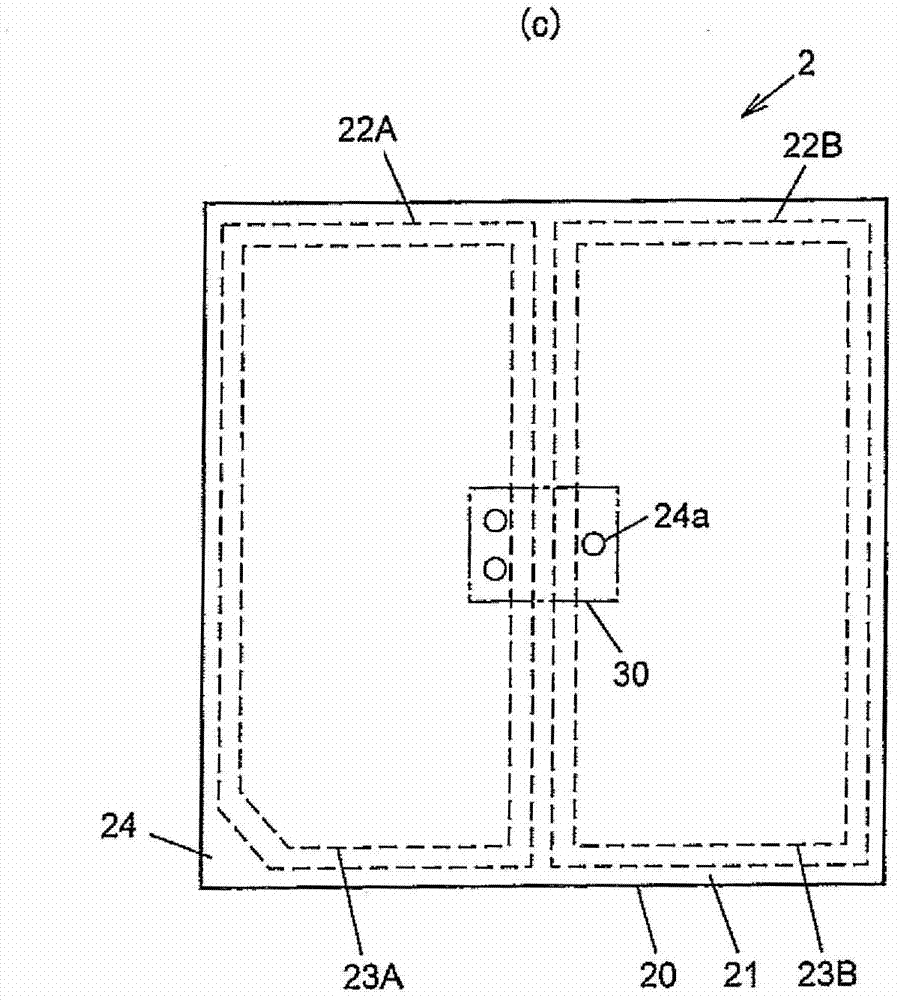
[0046] Figure 1A (a) is a cross-sectional view of the LED package according to the first embodiment of the present invention, Figure 1A (b) is from Figure 1A (a) Top view of the LED package with the sealing resin and insulating layer removed. Figure 1B (c) is a plan view of a substrate for mounting a light emitting element.

[0047] An LED package 1 as an example of a light emitting element such as Figure 1A As shown in (a) and (b), in the mounting region 30 of the pair of wiring patterns 22A, 22B of the light-emitting element mounting substrate 2, a flip-chip LED chip having electrodes 31a, 31b on the bottom surface as a light-emitting element is placed. 3 Perform flip-chip connection by bumps 32a and 32b, and seal the LED chip 3 with the sealing resin 4A.

[0048] The light-emitting element mounting substrate 2 is a so-called single-sided wiring board having wiring on one side of the substrate, and includes: a resin film 20 as a substrate having insulating properties; ...

no. 2 approach

[0120] Figure 4 (a) shows the LED package according to the second embodiment of the present invention, and is a plan view of the LED package with the sealing resin and insulating layer removed, Figure 4 (b) is a plan view of a substrate for mounting a light emitting element.

[0121] In the first embodiment, one LED chip 3 is mounted on the substrate 2 for mounting a light-emitting element, and the LED package 1 of this embodiment is as follows: Figure 4 As shown in (a), a plurality of (for example, three) LED chips 3 are mounted.

[0122] The mounting area 30 of this embodiment is an area including three LED chips 3 . The pair of wiring patterns 22A, 22B has a first distance d1 between the length of one side 30 a of the mounting region 30 , for example, 1.5 mm or more, and the length of one side 30 b of the mounting region 30 , for example, 0.04 mm or less.

[0123] The pair of filling portions 23A, 23B has a second distance d2 of, for example, 0.02 mm or less, within t...

no. 3 approach

[0126] Figure 5 (a) shows the LED package according to the third embodiment of the present invention, and is a plan view of the LED package without the sealing resin and the insulating layer, Figure 5 (b) is a plan view of a substrate for mounting a light emitting element.

[0127] In the first and second embodiments, there was only one mounting area 30 and only the flip-chip LED chip 3 was mounted. However, the present embodiment has a plurality of mounting areas 30A, 30B, and in addition to the LED chip 3, there are also Equipped with other electronic components.

[0128] That is, the LED package 1 of the present embodiment is as Figure 5 As shown in (a), a mounting region 30A is provided across a pair of wiring patterns 22A and 22B, and a mounting region 30B is also provided on one wiring pattern 22A. This LED package 1 mounts the same flip-chip LED chip 3 as in the first and second embodiments on one mounting area 30A, and mounts a wire-bonding LED chip 5A on the oth...


PUM


Abstract

A light-emitting element mounting substrate includes an insulative substrate including a single-sided printed circuit board, a pair of wiring patterns formed on one surface of the substrate, the wiring patterns being separated with a first distance, a pair of filled portions including a metal filled in a pair of through-holes to contact the pair of wiring patterns and to be exposed on a surface of the substrate opposite to the one surface, the pair of through-holes being formed to penetrate through the substrate in a thickness direction and to be separated with a second distance, and an insulation layer having a light reflectivity formed on the one surface of the substrate. The pair of filled portions each have a horizontal projected area of not less than 50% of each area the pair of wiring patterns, and the insulation layer includes an opening to expose the pair of wiring patterns.

Description

technical field [0001] The present invention relates to a substrate for mounting a light emitting element and an LED package using the substrate for mounting a light emitting element. Background technique [0002] In recent years, from the viewpoint of energy saving, display devices and lighting devices using LED (Light Emitting Diode) chips as light-emitting elements have attracted attention, and competition for the development of LED chips and related products and technologies has been aroused on a global level. . As a symbolic example, the price per unit brightness (yen / lm) is well known as an index. It can also be known from this unit that in order to win the competition, it is required to lower the price per unit or increase the beam per unit. [0003] Among them, as for LED chips, from the viewpoint of luminous efficiency, attention has been paid to flip-chip LED chips in which electrodes are provided on the back surface of the LED chip, as opposed to wire-bonded LED...

Claims


Application Information

Patent Timeline
Patent Type & Authority Applications(China)
IPC IPC(8): H01L33/64H01L33/60H01L33/62H01L33/48
CPCH01L25/0753H01L33/60H01L33/64H01L2224/48137H01L2224/45144H01L33/62H01L2224/48091H01L33/48H01L2224/48227H01L25/167H01L2924/00014H01L2924/00
Inventor 今井升伊坂文哉根本正德田野井稔高桥健
Owner SHINDOU DENSHI INDS
Why Eureka
Try Eureka