Processing method of through holes of printed circuit board (PCB) and through hole structure

A technology of a PCB board and a processing method is applied in the field of a PCB board through-hole processing method and through-hole structure for improving signal quality, which can solve the problems of large parasitic capacitance and affect the quality of high-speed signals, and achieves reduction of parasitic capacitance, low processing cost, The effect of improving transmission quality

Active Publication Date: 2013-01-16
NEW H3C TECH CO LTD
View PDF3 Cites 18 Cited by
  • Summary
  • Abstract
  • Description
  • Claims
  • Application Information

AI Technical Summary

Problems solved by technology

[0004] like figure 1 As shown in the figure, after the connector is pressed against both sides on the PCB, the diameter of the vacant metal aperture between the crimped pins is consis

Method used


Image

  • Processing method of through holes of printed circuit board (PCB) and through hole structure
  • Processing method of through holes of printed circuit board (PCB) and through hole structure
  • Processing method of through holes of printed circuit board (PCB) and through hole structure

Examples


Example Embodiment

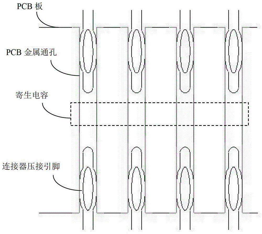
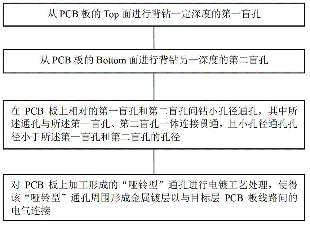
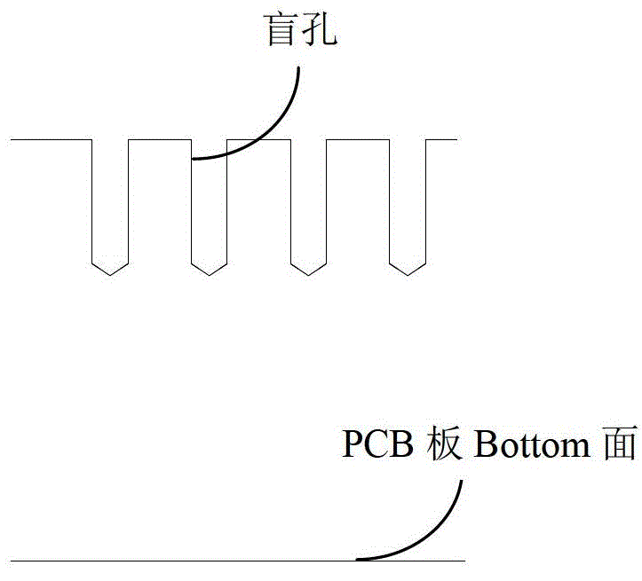
[0026] In order to achieve the purpose of the present invention, the core idea adopted by the present invention is: after the crimping device in the existing solution is pressed in the metal through hole of the PCB, a large parasitic capacitance is generated in the through hole, which affects the high speed in the PCB. The signal quality situation. The invention transforms the through-hole structure of the PCB board into a "dumbbell-shaped" structure. After the crimping device is pressed on the PCB board, since the vacant aperture between the crimping pins is much smaller than the through hole aperture in the existing solution, the parasitic capacitance generated is very small and the PCB signal quality is improved. The invention also provides a processing method for processing the "dumbbell-shaped" through-hole structure.

[0027] In order to make the technical solution of the present invention clearer and more comprehensible, a detailed description will be given below in conju...


PUM


Abstract

The invention discloses a processing method of through holes of a printed circuit board (PCB) and a through hole structure. The method and the structure aim at resolving the problem in the existing scheme that high speed signal quality in the PCB is affected by larger parasitic capacitance generated in the through holes after press connection devices are pressed mutually in the through holes of the PCB. By means of the method, the through hole structure of the PCB is modified and is processed into a 'dumbbell'-shaped structure. Therefore, the generated parasitic capacitance is very small after the press connection devices are mutually pressed on the PCB due to the fact that vacancy hole diameter between press connection pins is much smaller than that of the through holes in the existing scheme, and signal quality of the PCB is improved. The processing method of the 'dumbbell'-shaped through hole structure is further provided.

Description

technical field [0001] The invention relates to the technical field of communications, in particular to a PCB through-hole processing method and a through-hole structure for improving signal quality. Background technique [0002] As the signal rate of a single-layer PCB board becomes higher and higher, parasitic capacitance will be generated when the signal passes through the metal vias formed on the PCB board. Moreover, the larger the diameter of the metal via, the larger the generated parasitic capacitance. For high-speed signals, the existence of parasitic capacitance will delay the rising edge time of the signal. If the situation is relatively bad, it will cause serious crosstalk and signal transmission cannot continue. [0003] The technology of electrically connecting electronic components and PCB boards by crimping is becoming more and more widely used. It is mainly to design crimping pins that can be deformed by force on the device. When the crimping pins are press...

Claims


Application Information

Patent Timeline
IPC IPC(8): H05K3/00H05K3/42H05K1/11
Inventor 李义朱兴旺谈州明
Owner NEW H3C TECH CO LTD
Why Eureka
Try Eureka