Device and method for detecting micro-electronic packaging process quality based on photo-thermal imaging

一种图像获取装置、成像的技术,应用在测量装置、采用光学装置、光学测试瑕疵/缺陷等方向,达到降低刚度要求、检测评估可靠、结果可靠的效果

Active Publication Date: 2015-06-10
HUAZHONG UNIV OF SCI & TECH +1
View PDF9 Cites 0 Cited by
  • Summary
  • Abstract
  • Description
  • Claims
  • Application Information

AI Technical Summary

Problems solved by technology

[0003] However, limited by the constraints of feature size, micropore aspect ratio, etc., there are still many process problems to be solved in many TSV technology routes.

Method used


Image

  • Device and method for detecting micro-electronic packaging process quality based on photo-thermal imaging
  • Device and method for detecting micro-electronic packaging process quality based on photo-thermal imaging
  • Device and method for detecting micro-electronic packaging process quality based on photo-thermal imaging

Examples


Embodiment Construction

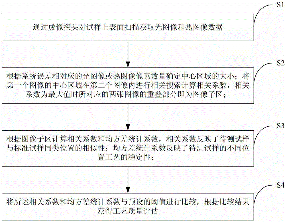
[0029] In order to make the object, technical solution and advantages of the present invention clearer, the present invention will be further described in detail below in conjunction with the accompanying drawings and embodiments. It should be understood that the specific embodiments described here are only used to explain the present invention, not to limit the present invention.

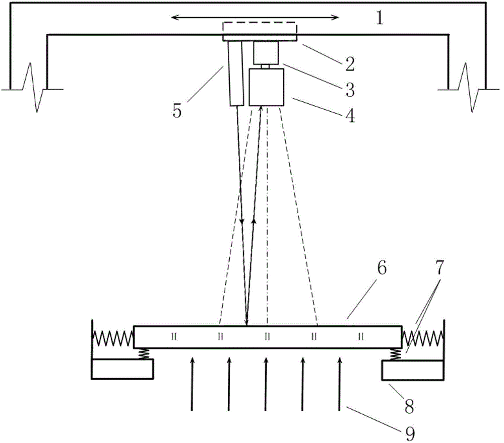
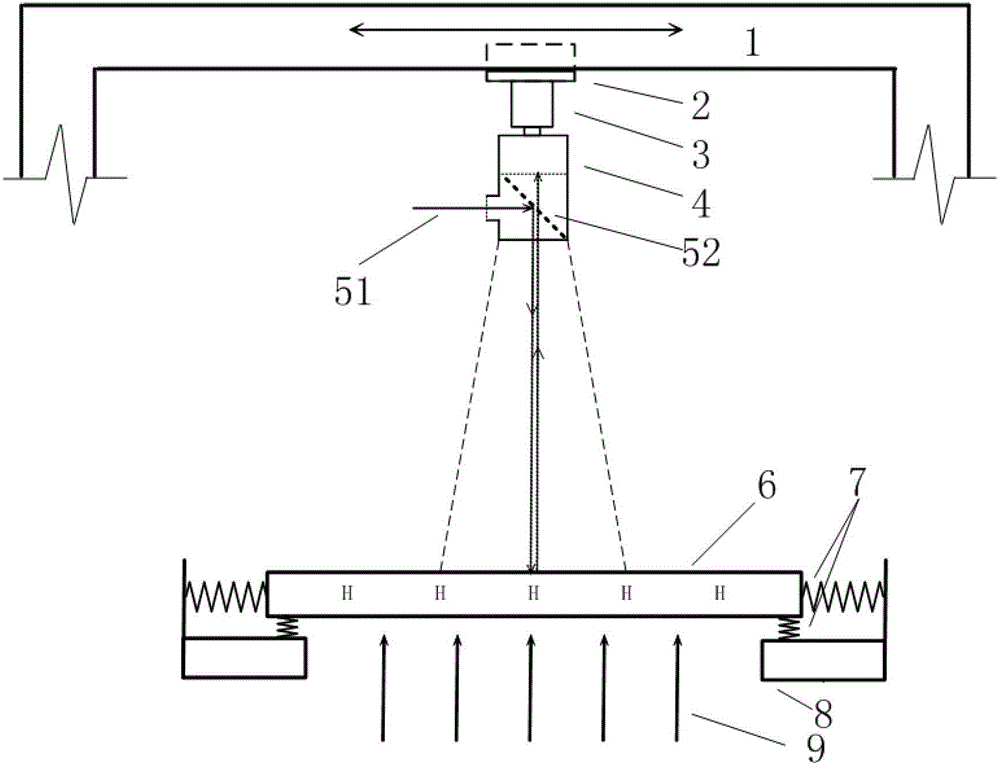
[0030] The invention provides a microelectronic packaging process quality detection device based on photothermal imaging, which can detect the process quality at different stages in the microelectronic packaging process flow; it is especially suitable for flip-chip, wafer-level packaging and three-dimensional integrated circuits based on silicon vias The quality inspection of semi-finished products and finished products at each stage of the process flow of packaging technology can also be used in advanced packaging processes such as embedded system-in-package, which helps to improve product yield an...


PUM


Abstract

An image acquisition device based on photo-thermal imaging, including a support beam, a translational electric motor, an imaging probe, and a light emitter. The translational electric motor is fixed to the lower side of the beam, and the imaging probe is perpendicularly fixed to a moving block in the translational electric motor. The light emitter is connected to the moving block via an adjustable connection piece, and by adjusting the adjustable connection piece, light emitted by the light emitter enters the imaging probe after being reflected by a sample. The moving block in the translational electric motor is configured to move the light emitter and the imaging probe in the radial direction right above the sample. The light emitter is configured to emit light on the upper surface of the sample. The imaging probe is configured to image reflected light from the upper surface of the sample.

Description

technical field [0001] The invention belongs to the field of microelectronic packaging, and more specifically relates to a photothermal imaging-based microelectronic packaging process quality detection device and method. Background technique [0002] Three-dimensional microelectronic packaging technology, that is, three-dimensional electronic packaging technology, is a higher-density electronic packaging that is further developed into space on the basis of two-dimensional planar electronic packaging. This technology can make the corresponding electronic system more functional, better in performance, and reliable. Higher reliability and lower cost. Among them, through-silicon via technology, as a new technology solution for interconnection of stacked chips in three-dimensional integrated circuits, has the following significant advantages: the stacking density of chips in the three-dimensional direction is the largest, the interconnection lines between chips are the shortest, ...

Claims


Application Information

Patent Timeline
Patent Type & Authority Patents(China)
IPC IPC(8): G01B11/00G01B11/22G01N15/14
CPCG01N21/95G01N25/72G01N21/55G01N2201/10G01N21/9501G01N2201/0636G01N2201/0638G01N2201/102
Inventor 刘胜戴宜全甘志银王小平
Owner HUAZHONG UNIV OF SCI & TECH
Why Eureka
Try Eureka