Device and method for detecting micro-electronic packaging process quality based on photo-thermal imaging

An image acquisition device and imaging technology, which are used in measurement devices, optical devices, optical testing of flaws/defects, etc., to achieve the effects of reliable detection and evaluation, reliable results, and easy accurate positioning and analysis

Active Publication Date: 2013-01-30
HUAZHONG UNIV OF SCI & TECH +1
View PDF9 Cites 13 Cited by
  • Summary
  • Abstract
  • Description
  • Claims
  • Application Information

AI Technical Summary

Problems solved by technology

[0003] However, limited by the constraints of feature size, micropore aspect ratio, etc., there are still many process problems to be solved in many TSV technology routes.

Method used


Image

  • Device and method for detecting micro-electronic packaging process quality based on photo-thermal imaging
  • Device and method for detecting micro-electronic packaging process quality based on photo-thermal imaging
  • Device and method for detecting micro-electronic packaging process quality based on photo-thermal imaging

Examples


Embodiment Construction

[0029] In order to make the object, technical solution and advantages of the present invention clearer, the present invention will be further described in detail below in conjunction with the accompanying drawings and embodiments. It should be understood that the specific embodiments described here are only used to explain the present invention, not to limit the present invention.

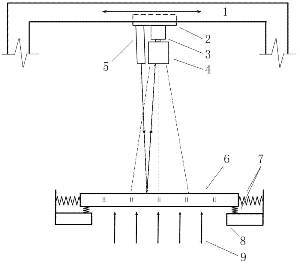
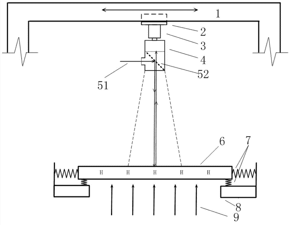
[0030] The invention provides a microelectronic packaging process quality detection device based on photothermal imaging, which can detect the process quality at different stages in the microelectronic packaging process flow; it is especially suitable for flip-chip, wafer-level packaging and three-dimensional integrated circuits based on silicon vias The quality inspection of semi-finished products and finished products at each stage of the process flow of packaging technology can also be used in advanced packaging processes such as embedded system-in-package, which helps to improve product yield an...


PUM


Abstract

The invention discloses a device for detecting micro-electronic packaging process quality based on photo-thermal imaging. The device for detecting the micro-electronic packaging process quality based on the photo-thermal imaging comprises an image acquiring device, a working bench, a control device and a data processing device, wherein the image acquiring device comprises a support cross beam, a translational motion motor, an imaging probe and a light transmitter. The translational motion motor is fixed on the lower lateral face of the cross beam, and the imaging probe is perpendicular to a moving block fixed in the translational motion motor. The light transmitter is connected to the moving block through an adjustable connecting piece, and emitted light is reflected by a sample and then enters the imaging probe by adjusting the adjustable connecting piece. The data processing device is used for processing light images and heat image data acquired by the image acquiring device to obtain correlation coefficient and mean square error statistic coefficient, comparing the correlation coefficient and the mean square error statistic coefficient and a preset threshold value and obtaining process quality evaluation according to a compared result. The device for detecting the micro-electronic packaging process quality based on the photo-thermal imaging can achieve recognition of residual particles, voids and material quality and measurement of microvoid depth and is reliable in detection and evaluation.

Description

technical field [0001] The invention belongs to the field of microelectronic packaging, and more specifically relates to a photothermal imaging-based microelectronic packaging process quality detection device and method. Background technique [0002] Three-dimensional microelectronic packaging technology, that is, three-dimensional electronic packaging technology, is a higher-density electronic packaging that is further developed into space on the basis of two-dimensional planar electronic packaging. This technology can make the corresponding electronic system more functional, better in performance, and reliable. Higher reliability and lower cost. Among them, through-silicon via technology, as a new technology solution for interconnection of stacked chips in three-dimensional integrated circuits, has the following significant advantages: the stacking density of chips in the three-dimensional direction is the largest, the interconnection lines between chips are the shortest, ...

Claims


Application Information

Patent Timeline
Patent Type & Authority Applications(China)
IPC IPC(8): G01B11/00G01B11/22G01N15/14
CPCG01N21/95G01N25/72G01N21/55G01N2201/10G01N21/9501G01N2201/0636G01N2201/0638G01N2201/102
Inventor 刘胜戴宜全甘志银王小平
Owner HUAZHONG UNIV OF SCI & TECH
Why Eureka
Try Eureka