A kind of graphene transfer annealing method and manufactured device based on Aln substrate

A graphene, single-layer graphene technology, applied in semiconductor/solid-state device manufacturing, electrical components, circuits, etc., can solve problems such as less experimental analysis, and achieve the advantages of suppressing doping effect, reducing residual amount, and optimizing annealing process. Effect

Inactive Publication Date: 2015-07-29
XIDIAN UNIV
View PDF4 Cites 0 Cited by
  • Summary
  • Abstract
  • Description
  • Claims
  • Application Information

AI Technical Summary

Problems solved by technology

Both methods can significantly remove residues or adsorbates on the graphene surface, but the focus of current research is mainly on SiO 2 / Si substrates, while there are few experimental analyzes on other substrates (such as AlN and other III-nitride wide bandgap semiconductor substrates)

Method used


Image

  • A kind of graphene transfer annealing method and manufactured device based on Aln substrate
  • A kind of graphene transfer annealing method and manufactured device based on Aln substrate

Examples


Embodiment 1

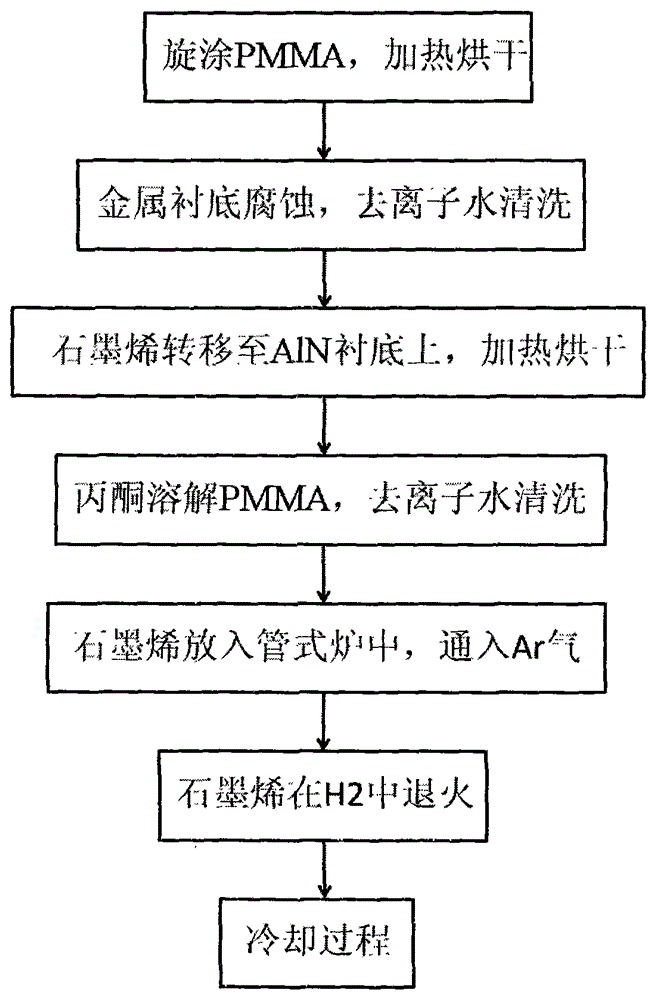
[0024] Fact steps of the present invention are as follows:

[0025] Step 1 Spin-coat a layer of PMMA on the graphene surface, heat the temperature to 60°C, and dry for 5 minutes;

[0026] Step 2 put the graphene into the ferric nitrate aqueous solution with a mass fraction of 10%, with the metal substrate layer facing down and the PMMA layer facing up until the metal layer is completely corroded, then cleaning with deionized water to remove the residual corrosion solution ;

[0027] Step 3 transfers the graphene / PMMA layer obtained in step (2) to an AlN substrate, and then bakes it for 20 minutes at a temperature of 60° C.;

[0028] Step 4 puts the PMMA / graphene / AlN substrate obtained in step (3) into an acetone solution to dissolve the PMMA, and then cleans it with deionized water;

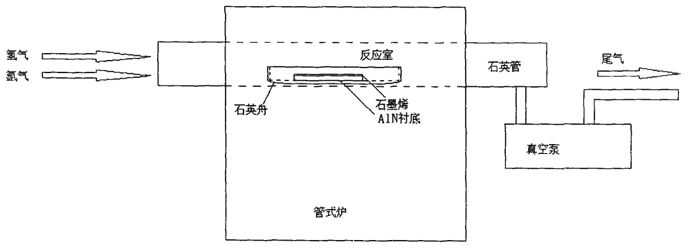
[0029] Step 5 Put the graphene transferred onto the AlN substrate into a tube furnace, vacuumize the tube furnace to 0.1Pa, and feed high-purity (purity > 99.9%) Ar gas into the tube furnace wi...

Embodiment 2

[0034] Fact steps of the present invention are as follows:

[0035] Step A Spin-coat a layer of PMMA on the graphene surface, heat the temperature to 50°C, and dry for 5 minutes;

[0036] Step B puts the graphene into the ferric nitrate aqueous solution with a mass fraction of 5%, with the metal substrate layer facing down and the PMMA layer facing up until the metal layer is completely corroded, then cleaning with deionized water to remove the residual corrosion solution ;

[0037] In step C, the graphene / PMMA layer obtained in step (2) is transferred to an AlN substrate, and then dried at 80° C. for 20 minutes;

[0038] Step D puts the PMMA / graphene / AlN substrate obtained in step (3) into an acetone solution to dissolve the PMMA, and then cleans it with deionized water;

[0039] Step E puts the graphene transferred onto the AlN substrate into a tube furnace, evacuates the tube furnace to 1Pa, and feeds high-purity (purity>99.9%) Ar gas into the tube furnace with a flow rat...

Embodiment 3

[0044] Fact steps of the present invention are as follows:

[0045] Step 1 Spin-coat a layer of PMMA on the graphene surface, heat to 80°C, and dry for 5 minutes;

[0046] Step 2 Put the graphene into a 20% ferric nitrate aqueous solution with the metal substrate layer facing down and the PMMA layer facing up until the metal layer is completely corroded, then clean it with deionized water to remove the residual corrosion solution ;

[0047] In step 3, the graphene / PMMA layer obtained in step (2) is transferred to an AlN substrate, and then dried at 60° C. for 40 minutes;

[0048] Step 4 puts the PMMA / graphene / AlN substrate obtained in step (3) into an acetone solution to dissolve the PMMA, and then cleans it with deionized water;

[0049] Step 5 Put the graphene transferred onto the AlN substrate into a tube furnace, vacuumize the tube furnace to 0.5 Pa, and feed high-purity (purity > 99.9%) Ar gas into the tube furnace with a flow rate of 150 sccm for 15 minutes , in order t...


PUM

PropertyMeasurementUnit
emission peakaaaaaaaaaa

Abstract

The invention discloses an AlN (aluminum nitride) substrate based graphene transfer and annealing method which is implemented through transferring large-area single-layer graphene to an AlN substrate by using a wet-process transfer method; and by way of low-pressure and low-temperature atmosphere annealing, adjusting the annealing temperature and the time of annealing treatment for the AlN substrate through optimizing atmosphere conditions so as to remove a PMMA (polymethyl methacrylate) residual photoresist in the process of transferring and reduce the doping effects of residues and the substrate on graphene as far as possible, thereby obtaining a graphene material with the optimal performance. By using the graphene subjected to transferring and annealing treatment, PMMA residues attached to the surface of the graphene can be removed better, and a good adhesion relation between the graphene and the substrate is kept well, thus the doping effects of adsorbates on the surface of the graphene and the substrate are minimized.

Description

technical field [0001] The invention belongs to the technical field of semiconductor materials and device manufacturing, and relates to a growth method for semiconductor materials, in particular to a graphene transfer annealing method based on an AlN substrate, which can be used for large-area high-quality graphene transfer and graphene devices with high electrical properties preparation. technical background [0002] Graphene is a two-dimensional crystal composed of carbon atoms. It is the lightest and thinnest material known so far, and it has very peculiar physical and chemical properties. For example, the extremely high carrier mobility (theoretical estimates exceed 200,000 cm 2 V -1 the s -1 , is hundreds of times that of Si), super mechanical properties (Young's modulus is about 1000GP), extremely high specific surface area and excellent gas-sensing properties, extremely high transparency and flexibility, and it is compatible with the substrate There is no mismatch...

Claims


Application Information

Patent Timeline
Patent Type & Authority Patents(China)
IPC IPC(8): H01L21/324H01L21/683
Inventor 宁静王东韩砀闫景东柴正张进成郝跃
Owner XIDIAN UNIV
Why Eureka
Try Eureka