Electronic devices and semiconductor substrates

A technology of electronic devices and semiconductors, applied in semiconductor devices, semiconductor/solid-state device manufacturing, lighting devices, etc., can solve problems such as threshold voltage and other electrical characteristics degradation, and achieve the effect of ensuring electrical characteristics

Inactive Publication Date: 2016-12-21
SONY CORP
View PDF7 Cites 0 Cited by
  • Summary
  • Abstract
  • Description
  • Claims
  • Application Information

AI Technical Summary

Problems solved by technology

This causes unexpected doping in the organic semiconductor layer, and therefore, electrical characteristics such as threshold voltage in the organic TFT tend to deteriorate

Method used


Image

  • Electronic devices and semiconductor substrates
  • Electronic devices and semiconductor substrates
  • Electronic devices and semiconductor substrates

Examples


Embodiment Construction

[0021] Hereinafter, embodiments of the present invention will be described in detail with reference to the accompanying drawings. Descriptions are given in the following order.

[0022] 1. Electronic device (organic EL display device) in the first embodiment

[0023] 2. Electronic device (liquid crystal display device) in the second embodiment

[0024] 1. Electronic device (organic EL display device) in the first embodiment

[0025] Structure of organic EL display device

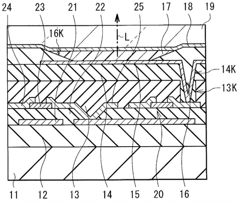
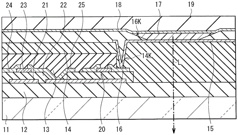
[0026] First, the electronic device according to the first embodiment of the present invention will be described. The electronic device here is an organic EL display device as an exemplary display device, and includes an organic TFT as a switching element. Please note that since the electronic device described here uses the semiconductor substrate of the embodiment of the present invention, the electronic device and the semiconductor substrate will be described together below.

[0027] figure 1 A cross...


PUM


Abstract

The present invention relates to semiconductor substrates and electronic devices. The semiconductor substrate includes: a thin film transistor including an organic semiconductor layer; and a light absorbing light transmitting layer disposed in a path that guides external light to the organic semiconductor layer. The light-absorbing light-transmitting layer absorbs light in a wavelength range including at least a part of the light-absorbing wavelength range of the organic semiconductor layer, and allows transmission of light in the remaining other wavelength ranges. The electronic device includes a light source, light generated from the light source as the external light, and the above-mentioned thin film transistor. The semiconductor substrate and the electronic device of the present invention can secure the electrical characteristics of the organic semiconductor layer.

Description

[0001] Cross References to Related Applications [0002] This application contains subject matter related to that disclosed in Japanese Priority Patent Application JP 2011-183985 filed in Japan Patent Office on Aug. 25, 2011, the entire content of which is hereby incorporated by reference. technical field [0003] The present invention relates to a semiconductor substrate provided with a thin film transistor including an organic semiconductor layer and an electronic device using the semiconductor substrate. Background technique [0004] In recent years, various electronic devices use a thin film transistor (TFT) as a switching element and the like, and the TFT is mounted on the electronic device as a part of a semiconductor substrate. Regarding TFTs, an organic TFT that uses an organic semiconductor material to form a semiconductor layer (channel layer) has recently been considered as a promising alternative to an inorganic TFT that uses an inorganic semiconductor material t...

Claims


Application Information

Patent Timeline
Patent Type & Authority Patents(China)
IPC IPC(8): H01L51/05H01L51/10H01L27/32G02F1/1368G02F1/13357H05B44/00
CPCG02F1/133602G02F2202/02G02F2203/055H10K59/126H10K10/466
Inventor 胜原真央汤本昭
Owner SONY CORP
Why Eureka
Try Eureka