Method for controlling aperture size of via hole on TFT substrate

A technology of aperture size and via hole, which is applied in the field of display screens, can solve the problems of enlarged aperture, fluctuation, and influence on the electrical characteristics of lap resistance, etc., to achieve enhanced control, ensure lap resistance and electrical characteristics, and avoid backing phenomenon Effect

Pending Publication Date: 2022-02-18
TRULY HUIZHOU SMART DISPLAY
View PDF0 Cites 0 Cited by
  • Summary
  • Abstract
  • Description
  • Claims
  • Application Information

AI Technical Summary

Problems solved by technology

During the etching process, the change of the aperture size of the via hole will affect the electrical characteristics of the TFT, which will directly affect the display effect, reliability and yield of the product.
[0004] Via etching in existing TFT substrates generally uses photoresist (Photo Resist, PR) as a mask to pass CF 4 、C 4 f 8 、C 2 HF 5 Or other fluorine-containing gas ionization for dry etching, but because of the thickness of the PR glue, slope angle and etching uniformity, the PR will retreat, that is, the pore size will become larger, the CD LOSS cannot be effectively controlled, and there will be fluctuations. Thus affecting the bonding resistance and electrical characteristics

Method used


Image

  • Method for controlling aperture size of via hole on TFT substrate
  • Method for controlling aperture size of via hole on TFT substrate

Examples


Embodiment Construction

[0025] It should be understood that the specific embodiments described here are only used to explain the present invention, not to limit the present invention.

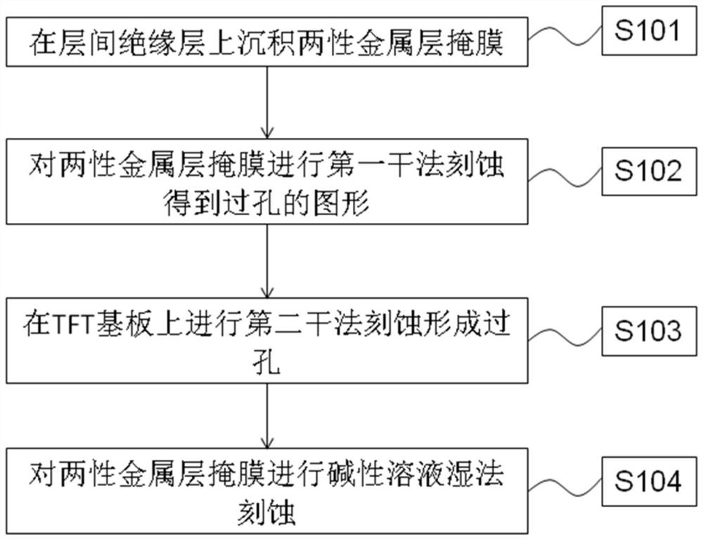
[0026] Such as figure 1 As shown, a method for controlling the size of the via hole on the TFT substrate, comprising:

[0027] S101: Depositing an amphoteric metal layer mask on the interlayer insulating layer;

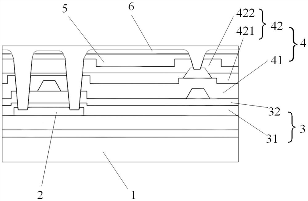
[0028] The amphoteric metals include aluminum and zinc, and aluminum has a price advantage in raw material cost. In this embodiment, preferably, the amphoteric metal is aluminum, and the amphoteric metal layer mask is an aluminum layer mask. Such as figure 2 As shown, the TFT substrate structure from top to bottom is photoresist 6, aluminum layer mask 5, SiN x The second interlayer insulating layer 422, SiO x The second interlayer insulating layer 421, the first interlayer insulating layer 41, SiN x Gate insulating layer 32, SiO x The gate insulating layer 31, the active layer 2, and the aluminum layer...


PUM

PropertyMeasurementUnit
thicknessaaaaaaaaaa

Abstract

The invention relates to a method for controlling the aperture size of a via hole on a TFT substrate, the via hole penetrates through an interlayer insulating layer and a gate insulating layer, and the method comprises the following steps: depositing an amphoteric metal layer mask on the interlayer insulating layer; performing first dry etching on the amphoteric metal layer mask to obtain a pattern of a via hole; performing second dry etching on the TFT substrate to form a via hole; and carrying out alkaline solution wet etching on the amphoteric metal layer mask. According to the method provided by the invention, the retreating phenomenon is avoided, and the control on the aperture size is effectively enhanced, so that the CD LOSS is controlled, and the overlapping resistance and the electrical characteristic of a product are ensured.

Description

technical field [0001] The invention relates to the technical field of display screens, in particular to a method for controlling the diameter of via holes on a TFT substrate. Background technique [0002] At present, in the display field, whether it is liquid crystal display technology or active matrix organic light-emitting diodes, the application in the display requires Thin Film Transistor (Thin Film Transistor, TFT) technology as the backplane driving technology. The control of the liquid crystal molecular matrix of a specific pixel realizes the control of the liquid crystal display; in the active matrix organic light-emitting diode display, the pixel display is realized through the individual control of the specific pixel light-emitting diode by TFT. [0003] Low temperature polysilicon (Low Temperature Poly-silicon, LTPS) technology has become a new generation of TFT manufacturing technology. In the application of LTPS technology to manufacture TFT substrates, the pr...

Claims


Application Information

Patent Timeline
Patent Type & Authority Applications(China)
IPC IPC(8): H01L21/77H01L27/12
CPCH01L27/1288H01L27/1214
Inventor 肖子黎冼伟材刘伟李伟界戴成云
Owner TRULY HUIZHOU SMART DISPLAY
Why Eureka
Try Eureka