Test structure, wafer and manufacturing method of test structure

A technology of testing structure and manufacturing method, applied in semiconductor/solid-state device testing/measurement, semiconductor/solid-state device manufacturing, semiconductor/solid-state device components, etc., to achieve the effect of improving yield and reliability

Active Publication Date: 2020-11-03
GIGADEVICE SEMICON SHANGHAI INC +1
View PDF6 Cites 0 Cited by
  • Summary
  • Abstract
  • Description
  • Claims
  • Application Information

AI Technical Summary

Problems solved by technology

[0004] The shielding effect is related to the direction of ion implantation and the thickness of the photoresist. Due to space constraints in the layout of the memory circuit, the same circuit will be configured in different directions, resulting in the electrical characteristics of the actual integrated circuit structure being affected by the ion implantation. There are differences in different directions. In order to monitor the electrical characteristics in the actual integrated circuit structure, the present invention provides a test structure for semiconductor integrated circuits that can reflect the parasitic conditions of circuit components in all directions and the shadow effect of ion implantation.

Method used


Image

  • Test structure, wafer and manufacturing method of test structure
  • Test structure, wafer and manufacturing method of test structure
  • Test structure, wafer and manufacturing method of test structure

Examples


Embodiment Construction

[0029] Various embodiments of the invention will be described in more detail below with reference to the accompanying drawings. In the various drawings, the same elements are denoted by the same or similar reference numerals. The components in the drawings are only for illustration, and do not have actual size proportional relationship. It should be noted that, in the case of no conflict, the embodiments in the present application and the features in the embodiments can be combined arbitrarily with each other.

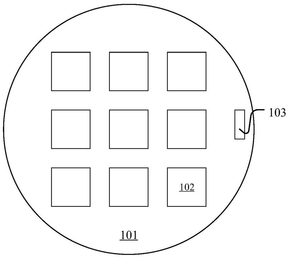
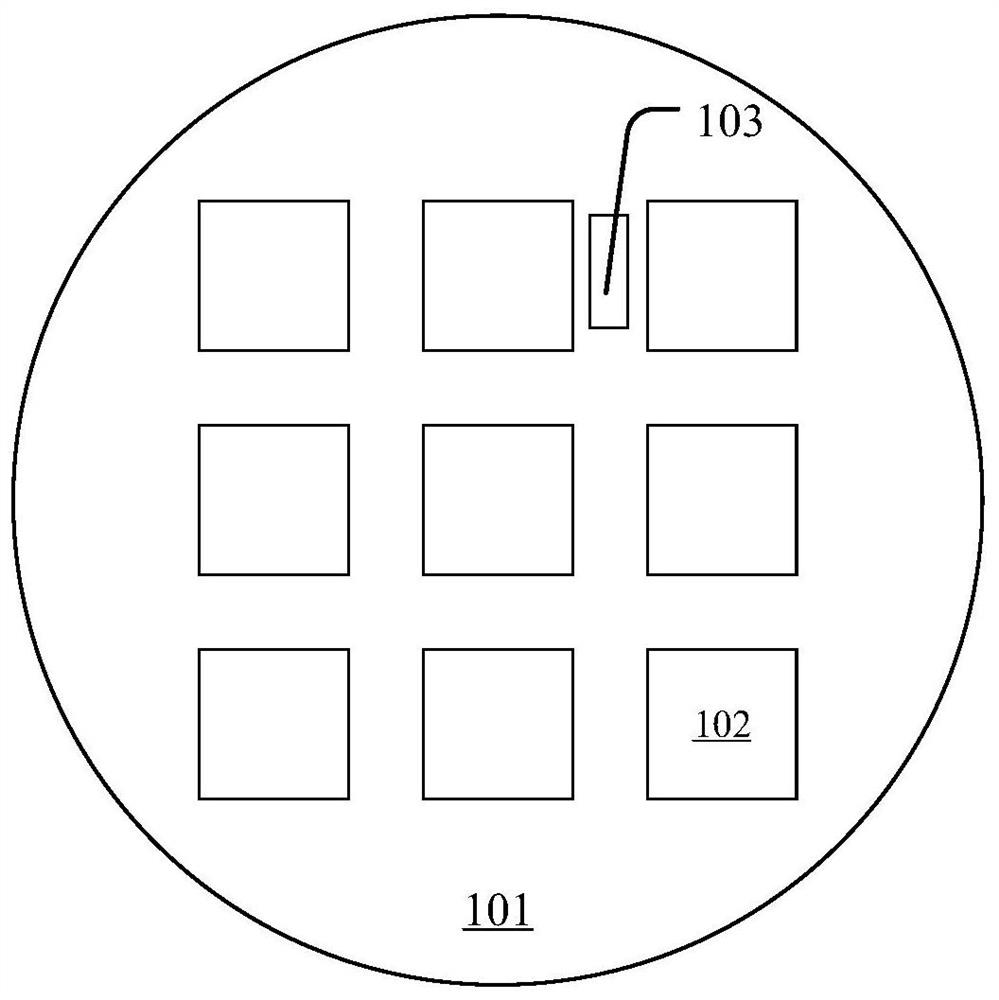
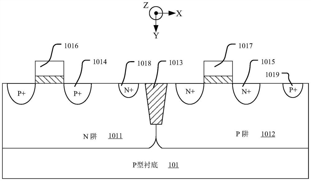
[0030] The manufacture of integrated circuits needs to form a large number of circuit components on a specific substrate area according to the specified circuit layout, such as multiple NMOS and PMOS. In order not to affect the performance of integrated circuits, isolation between adjacent circuit components is required. Corresponding Yes, it is also necessary to monitor the isolation of integrated circuits, such as parasitic PN junctions or parasitic BJTs in integrat...


PUM


Abstract

The invention discloses a test structure of an integrated circuit, and the structure comprises a plurality of groups of first doping fingers and a plurality of groups of second doping fingers, whereinat least one group of first doping fingers and at least one group of second doping fingers are arranged in an interdigital configuration in a first direction, at least one group of the first doping fingers and at least one group of the second doping fingers are arranged in an interdigital configuration in a second direction, and the first direction is perpendicular to the second direction. According to the test structure of the integrated circuit, the breakdown characteristics of parasitic junctions in different directions in the chip can be detected, and meanwhile, the influence caused by ashielding effect can be considered, so the complexity in the manufacturing process of the integrated circuit is better monitored, and the yield and the reliability of a semiconductor integrated circuit are improved.

Description

technical field [0001] The invention relates to the technical field of integrated circuits, in particular to a test structure, a manufacturing method of the test structure, and a wafer. Background technique [0002] The fabrication of integrated circuits requires the formation of a large number of circuit components on a specific substrate area according to a specified circuit layout. CMOS is formed in millions in integrated circuits due to its superior characteristics in both operation speed and cost efficiency. [0003] A flash memory (Flash) chip needs to use a voltage much higher than the power supply voltage when performing read, write and erase operations (for example, a flash memory chip may use a positive high voltage of +11V and a negative high voltage of -11V), which leads to the device in the flash memory chip Internal and / or isolation requirements between different devices are getting higher and higher. This requirement not only includes the design of the device...

Claims


Application Information

Patent Timeline
Patent Type & Authority Applications(China)
IPC IPC(8): H01L23/544H01L21/265
CPCH01L22/30H01L21/265
Inventor 刘钊熊涛许毅胜
Owner GIGADEVICE SEMICON SHANGHAI INC
Why Eureka
Try Eureka