Process for improving isolating oxide chemical mechanical planarization (CMP) uniformity

A technology for isolating oxides and uniformity, which is applied in the manufacture of electrical components, circuits, semiconductors/solid-state devices, etc. It can solve problems such as thickness differences, device defects, and reduced CMP uniformity, so as to reduce height differences, increase windows, Effect of improving planarization uniformity

Active Publication Date: 2013-03-13
BEIJING YANDONG MICROELECTRONICS
View PDF4 Cites 4 Cited by
  • Summary
  • Abstract
  • Description
  • Claims
  • Application Information

AI Technical Summary

Problems solved by technology
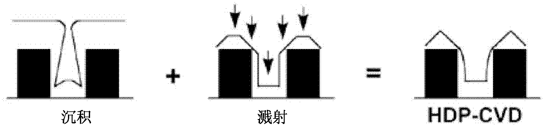
[0005] All in all, when the current HDP-CVD fills the isolation oxide structure with high AR, the large silicon oxide thickness difference reduces the CMP uniformity and causes device defects

Method used


Image

  • Process for improving isolating oxide chemical mechanical planarization (CMP) uniformity
  • Process for improving isolating oxide chemical mechanical planarization (CMP) uniformity
  • Process for improving isolating oxide chemical mechanical planarization (CMP) uniformity

Examples


Embodiment Construction

[0020] The features and technical effects of the technical solution of the present invention will be described in detail below with reference to the accompanying drawings and in conjunction with exemplary embodiments, and a method for improving the uniformity of the isolation oxide CMP is disclosed. It should be pointed out that similar reference signs indicate similar structures. The terms "first", "second", "upper", "lower", etc. used in this application can be used to modify various device structures or process steps. . Unless otherwise specified, these modifications do not imply the spatial, order, or hierarchical relationship of the modified device structure or process steps.

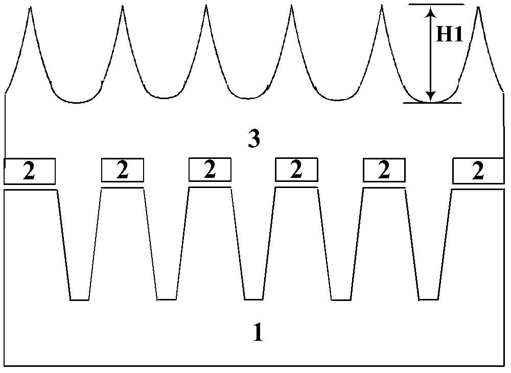
[0021] First, refer to figure 2 , Form the basic structure. The basic structure includes a substrate 1, a pad layer 2 on the substrate 1, and an isolation oxide layer (gap fill) 3 on the pad 2 and partially in the substrate 1. The substrate 1 is, for example, bulk silicon, silicon-on-insulator (SOI...


PUM


Abstract

The invention discloses a process for improving isolating oxide CMP uniformity. The process comprises the steps of forming a cushion layer on a substrate, and forming isolating oxide layers on the cushion layer and in the substrate; forming first covering layers on isolating oxide layers, wherein the height difference between tops of first covering layers is equal to or lager than that between tops of isolating oxide layers; forming second covering layers on first covering layers, wherein the height difference between tops of second covering layers is smaller than that between tops of first covering layers and / or that between tops of isolating oxide layers; and conducting CMP treatment on second covering layers, first covering layers and isolating oxide layers sequentially till the cushion layer is exposed. According to the process, integration is conducted in a process chamber of high-density plasma (HDP) depositions, no additional process step is required, the filling effect can be guaranteed at the same time when height differences are effectively reduced, and dishing defects in the CMP process can be reduced or avoided, so that the planarization uniformity of the CMP process can be improved, and the window of the CMP process can be expanded.

Description

Technical field [0001] The present invention relates to a method for manufacturing a semiconductor device, in particular to a method for improving the uniformity of isolation oxide chemical mechanical planarization (CMP). Background technique [0002] Since the introduction of shallow trench isolation (STI) technology from the 0.25um technology node, high-density isolation of devices has become possible. As technology nodes continue to shrink, in order to improve device density and isolation effects, the aspect ratio (AR) of the shallow trench itself continues to increase. High-density plasma chemical vapor deposition (HDP-CVD) is the mainstream technology for filling shallow trenches. This technology overcomes the sealing problem that may exist on the top of the trench through the cyclic process of etching while depositing. Silicon oxide is used to complete the filling of the large AR trench structure, which combines deposition and sputtering to complete the process. See attach...

Claims


Application Information

Patent Timeline
Patent Type & Authority Applications(China)
IPC IPC(8): H01L21/3105H01L21/762
Inventor 王桂磊杨涛李俊峰赵超
Owner BEIJING YANDONG MICROELECTRONICS
Why Eureka
Try Eureka