Ball grid array manufactured on printed circuit board

A technology for printed circuit boards and ball grid arrays, applied in the field of ball grid arrays, can solve the problems of wasting printed circuit board area, difficult to reuse ball grid arrays, and labor-intensive ball grid arrays.

Active Publication Date: 2013-03-13
MEDIATEK INC
View PDF4 Cites 2 Cited by
  • Summary
  • Abstract
  • Description
  • Claims
  • Application Information

AI Technical Summary

Problems solved by technology

[0003] As mentioned above, because the traditional BGA volleyball method has no fixed pattern, and the arrangement of solder balls is relatively scattered, the area of ​​the printed circuit board will be wasted, and the design of the BGA is not easy to be reused, and it also requires a lot of work. manpower to determine the performance of the ball grid array

Method used


Image

  • Ball grid array manufactured on printed circuit board
  • Ball grid array manufactured on printed circuit board
  • Ball grid array manufactured on printed circuit board

Examples


Embodiment Construction

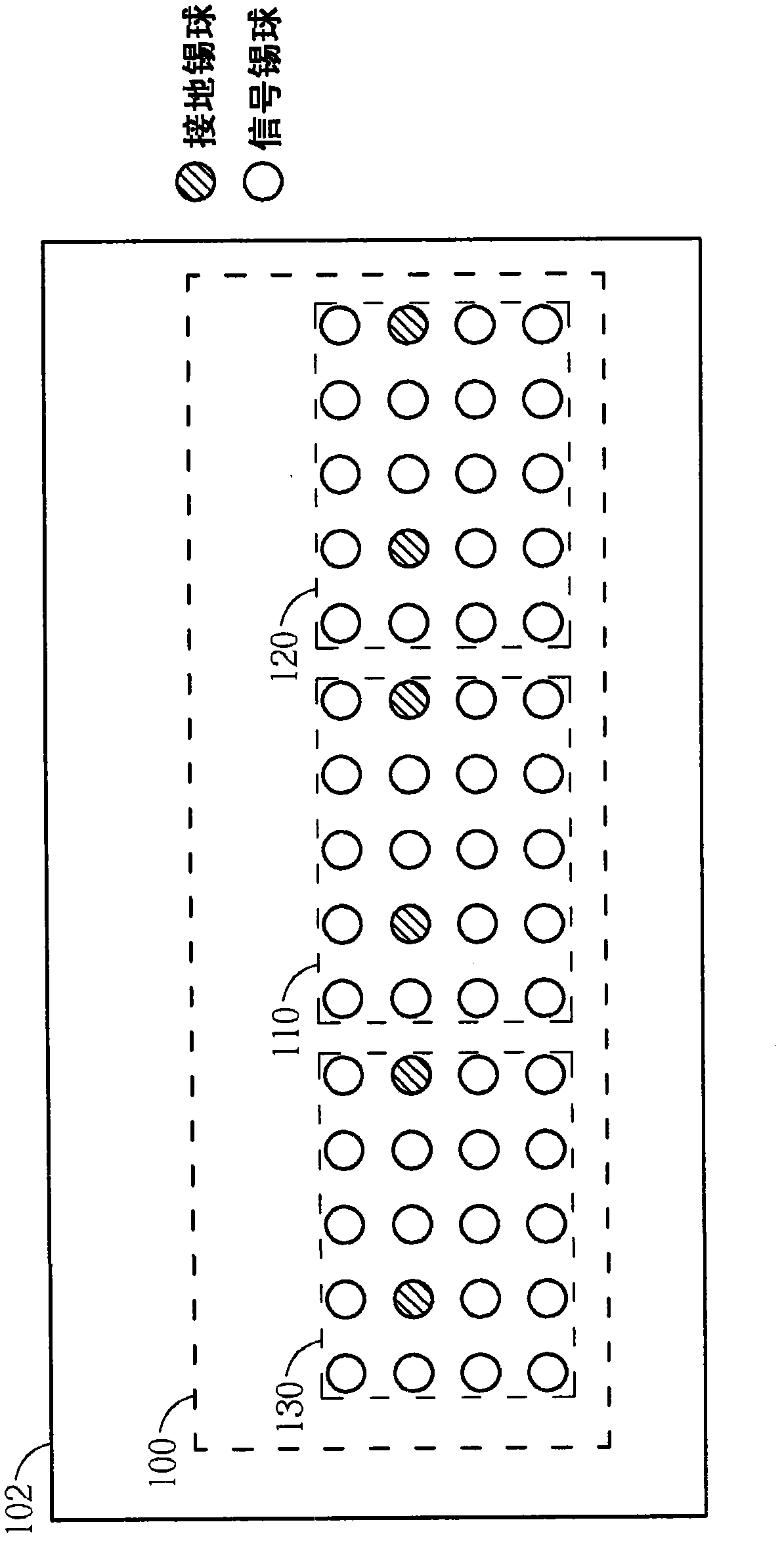
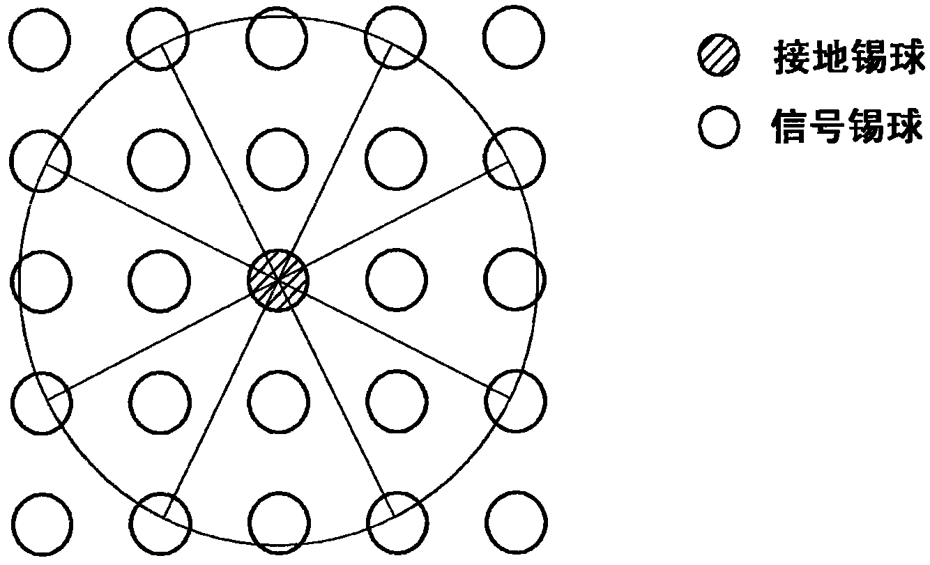
[0019] Please refer to figure 1 , figure 1 It is a schematic diagram of a ball grid array 100 fabricated on a printed circuit board 102 according to an embodiment of the present invention. Such as figure 1 As shown, the ball grid array 100 includes a first solder ball module 110, a second solder ball module 120 and a third solder ball module 130, wherein the first, second and third solder ball modules 110, 120, 130 have The same solder ball arrangement pattern. Each solder ball module includes twenty solder balls arranged in a 4*5 array, that is, each row of each solder ball module has five solder balls, and each row (column) has four solder balls. Only two solder balls in each solder ball module are grounded, and the two grounded solder balls are located in the third column of the solder ball module. The first column of the solder ball modules (ie, the lowest column of the ball grid array 100 ) faces the signal input lines input to the solder ball modules on the printed c...


PUM


Abstract

The invention discloses a ball grid array manufactured on a printed circuit board. The ball grid array comprises a first solder ball module and a second solder ball module. The first solder ball module comprises a plurality of first solder balls arranged into an array, two of the plurality of the first solder balls are earthed, and the other first solder balls are placed in a range shielded by the two earthed solder balls; the second solder ball module is arranged in parallel with the first solder ball module and comprises a plurality of second solder balls, two of the plurality of the second solder balls are earthed, and the other second solder balls are placed in a range shielded by the two earthed solder balls; and solder ball arranging modes of the first solder ball module and the second solder ball module are identical in essence in regard to relative positions of the two earthed solder balls and the other solder balls which are not earthed.

Description

technical field [0001] The present invention relates to a ball grid array disposed on a printed circuit board, especially a ball grid array with good ground shielding. Background technique [0002] In order to electrically connect a chip packaged with a ball grid array (BGA) to a printed circuit board, a ball grid array corresponding to the packaged chip will be provided on the printed circuit board, wherein the ball grid array is composed of a plurality of solder balls constituted, and among the plurality of solder balls, a few solder balls are grounded to provide ground shielding for other solder balls. However, generally speaking, the arrangement of the BGAs on the printed circuit board does not have certain rules, that is, the shape of the BGAs and the number and positions of the solder balls grounded will vary with different chips. [0003] As mentioned above, because the volleyball method of the traditional ball grid array has no fixed type, and the arrangement of the...

Claims


Application Information

Patent Timeline
IPC IPC(8): H05K1/02H05K1/11H05K3/46
Inventor 许健丰田尔文王挺光
Owner MEDIATEK INC
Why Eureka
Try Eureka