

Organic semiconductor material and application thereof in organic light-emitting diode (OLED) device
A technology of organic semiconductors and devices, which is applied in the field of organic semiconductor materials, can solve the problems of low conductivity, reduce the life and stability of OLED devices, and PVK hole injection/transport performance is not very good, so as to achieve high conductivity and avoid adverse effects
- Summary
- Abstract
- Description
- Claims
- Application Information
AI Technical Summary
Problems solved by technology
Method used
Image

Examples
Embodiment 1
[0022] Preparation of 4,4-dibromo-2-nitrobiphenyl (1)
[0023] Dissolve 4,4-dibromobiphenyl (20g, 64mmol) in glacial acetic acid (300mL), heat and stir at 110°C, add concentrated nitric acid (70%, 132mL) dropwise to glacial acetic acid, heat for 6h until solid Slowly dissolve, then cool to room temperature. The reaction solution was filtered, the solid was washed with water, and then recrystallized with ethanol to obtain a yellow solid (17.6g, yield77%). 1 H-NMR (300MHz, CDCl 3 ): (ppm) 8.32 (d, 2H), 8.29 (d, 2H), 7.77 (dd, 2H).
Embodiment 2
[0025] Preparation of 2,7-dibromocarbazole (2)
[0026] Triethyl phosphate (60 mL) added with compound 1 (16.5 g, 46.1 mmol) was heated to reflux for 18 h under nitrogen protection. The reaction solution was distilled off under reduced pressure to remove excess solvent, and the residue was dissolved in a small amount of dichloromethane, then precipitated with petroleum ether to obtain the initial product, and then silica gel / petroleum ether column chromatography was used to obtain a white solid (9.28g, yield 62%). 1 H-NMR (300MHz, CDCl 3 ): δ (ppm) 8.20 (br, 1H, NH); 7.92 (d, 2H); 7.56 (d, 2H); 7.35 (dd, 2H).
Embodiment 3
[0028] Preparation of p-methylphenyl-1-bromo-6-hexyl ether (3)
[0029] Add p-cresol (28g), 1,6-dibromohexane (220mL), potassium carbonate (60g), tetrabutylammonium bromide (3.8g) and acetone (150mL) into a 500mL flask, heat and stir to reflux 48h. The reaction was cooled to room temperature, filtered, and the filtrate was spun with a circulating water pump until the mass was no longer reduced, then distilled under reduced pressure with an oil pump, and the fraction collected at 210°C to 220°C was a colorless oily product (53.5g, yield76.1%). 1 H-NMR (300MHz, CDCl 3 ): δ (ppm) 7.10 (d, 2H); 6.82 (d, 2H); 3.96 (t, 2H); 3.45 (t, 2H); 2.32 (s, 3H); 1.8 (br, 8H).
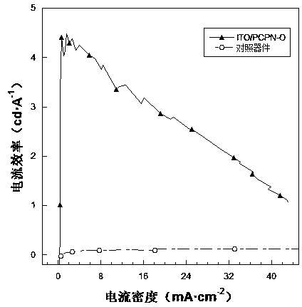
PUM
| Property | Measurement | Unit |
|---|---|---|
| current efficiency | aaaaa | aaaaa |
| current efficiency | aaaaa | aaaaa |
Abstract
Description
Claims
Application Information